
Fig 5. NPN Transistorbiased with a "base bias" resistor and a LOAD resistor
| Fig 5 shows an NPN transistor in SELF BIAS mode. This is called a COMMON EMITTER stage and the resistance of the BASE BIAS RESISTOR is selected so the voltage on the collector is half-rail voltage. In this case it is 2.5v.
To keep the theory simple, here's how you do it. Use 22k as the load resistor.
Select the base bias resistor until the measured voltage on the collector is 2.5v. The base bias resistor will be about 2M2.
This is how the transistor gets turned on by the base bias resistor:
The base bias resistor feeds a small current into the base and this makes the transistor turn ON and creates a current-flow though the collector-emitter leads.
This causes the same current to flow through the load resistor and a voltage-drop is created across this resistor. This lowers the voltage on the collector.
The lower voltage causes a lower current to flow into the base, via the base-bias resistor, and the transistor stops turning on a slight amount. The transistor very quickly settles to allowing a certain current to flow through the collector-emitter and produce a voltage at the collector that is just sufficient to allow the right amount of current to enter the base. That's why it is called SELF BIAS. |
 Fig 6. Turning ON an NPN transistor Fig 6. Turning ON an NPN transistor
| Fig 6 shows the transistor being turned on via a finger. Press hard on the two wires and the LED will illuminate brighter. As you press harder, the resistance of your finger decreases. This allows more current to flow into the base and the transistor turns on harder. |
 Fig 7. Two transistors turning ON Fig 7. Two transistors turning ON
| Fig 7 shows a second transistor to "amplify the effect of your finger" and the LED illuminates about 100 times brighter. |
 Fig 8. Adding a capacitor Fig 8. Adding a capacitor
| Fig 8 shows the effect of putting a capacitor on the base lead. The capacitor must be uncharged and when you apply pressure, the LED will flash brightly then go off. This is because the capacitor gets charged when you touch the wires. As soon as it is charged, NO MORE CURRENT flows though it. The first transistor stops receiving current and the circuit does not keep the LED illuminated. To get the circuit to work again, the capacitor must be discharged. This is a simple concept of how a capacitor works. A large-value capacitor will keep the LED illuminated for a longer period of time as it will take longer to charge. |
 Fig 9. Adding a capacitor to the output Fig 9. Adding a capacitor to the output
| Fig 9 shows the effect of putting a capacitor on the output. It must be uncharged for this effect to work. We know from Fig 7 that the circuit will stay ON constantly when the wires are touched but when a capacitor is placed in the OUTPUT, it gets charged when the circuit turns ON and only allows the LED to flash.
The electrolytic must be manually discharged to see the effect again. |
1. This is a simple explanation of how a transistor works. It amplifies the current entering the base (about 100 times) and the higher current flowing through the collector-emitter leads will illuminate a LED or drive other devices.
2. A capacitor allows current to flow through it until it gets charged. It must be discharged to see the effect again. |
TRANSISTOR PINOUTS:
 Transistor Pinouts Transistor Pinouts
| Just some of the pinouts for a transistor. You need to refer to a data sheet or test the device to determine the pins as there are NO standard pin-outs. |
THE RESISTOR
Before we go any further, we need to talk about the RESISTOR.
It's a two-leaded electrical component that has resistance from a fraction of an OHM to many millions of ohms (depending how much carbon is in the resistor). When the resistance is very low (small) the resistor is equal to a piece of wire and when it is very high, the resistance is equal to . . . . . .
The value of a resistor is marked on the body with bands of colours or, in the case of surface-mount resistors, a set of numbers. These identify the value of the resistor in OHMs. When the value of resistance is above one-thousand ohms, we use the letter "k" - for example 1,200 ohms is 1.2k or 1k2. When the value is above one-million ohms, we use the letter "M" - for example 2,200,000 ohms is 2.2M or 2M2. When the value is say 100 ohms we use the letter "R" - 100R.
Resistors do "all kinds of things" in a circuit. In other words, they can join two components, separate two components, prevent a component from getting too hot, prevent an amplifier from overloading, allow a capacitor to charge quickly or slowly - and many more.
All these things can be achieved because a resistor has ONE SIMPLE FEATURE . . .
A resistor limits (or reduces) the current-flow.
That's all a resistor does. It limits - or controls - or allows - a current to flow according to the resistance of the resistor.
This simple feature of limiting the current is like a man with a hammer - he can hammer nails, break glass, drive a pole into the ground and lots more and a resistor can do more than 12 different "things."
When a current flows through a resistor, a voltage is developed across it. This voltage is called the VOLTAGE DROP. (It is also called the VOLTAGE LOST ACROSS THE RESISTOR).
The following 3 examples will help you understand the terms VOLTAGE DROP and VOLTAGE LOST.

In diagram A, the resistor is only connected at one end and NO CURRENT will flow. This means the VOLTAGE DROP across the resistor will be ZERO. 12v is present on the lower lead of the resistor because no current is flowing.
In diagram B, the resistor is connected to a glowing lamp and current will flow. The voltage across the resistor may be 3v. In other words, the voltage LOST is 3v and the lamp gets only 9v. We also say theVOLTAGE DROP is 3v across the resistor.
In diagram C, the resistor is connected across the power rails and the voltage across it MUST be 12v. We do not talk about voltage drop or voltage lost in this circuit because there are no other components. We just say: the voltage across the resistor is 12v.
This will help you understand how a resistor works.
THE VOLTAGE DIVIDERNearly ALL circuits (and individual stages) use a VOLTAGE DIVIDER. A Voltage Divider is simply two resistors connected in series.
However it may not be two resistors. It may be a resistor and a transistor. A transistor is really a resistor - a variable resistor - and they form a voltage divider with a resistor called the LOAD. Sometimes more resistors are present (such as resistors creating an H-bridge biasing network) and there may be more than one voltage divider in a stage.
However the same principle applies.
The principle is this:
CURRENT FLOWS THROUGH THE COMBINATION (the current is the same for each resistor because they are in series).
Multiply the current (in amps) by the resistance (in ohms) to get the voltage across each resistor.
In most cases, the sum of the voltages across each resistor must add up to the supply voltage.
Here are 2 examples of a VOLTAGE DIVIDER:

This is as far as we can go without using mathematics.
A "STAGE"
A "Stage" is a set of components with a capacitor at the input and a capacitor on the output.
We have already seen the fact that the capacitor only has an effect on the circuit during the time when it gets charged. It also has an effect when it gets discharged. But when the voltage on either lead does not rise or fall, NO CURRENT flows through the capacitor.
When a capacitor is placed between two stages, it gradually charges. When it is charged, the voltage on one stage does not affect the voltage on the next stage. That's why the capacitor is drawn as two lines with a gap. A capacitor is like putting a magnet on one side of a door and a metal sheet on the other. Moving the magnet up and down will move the metal up and down but the two items never touch.
Only a rising and falling voltage is able to pass through the capacitor.
|
 Fig 10. This is a STAGE. Fig 10. This is a STAGE.
A transistor, with a capacitor
on the input and output.
| Fig 10 has a capacitor on the input and output. This means the stage is separated from anything before it and anything after it as far as the DC voltages are concerned and the transistor will produce its own operating point via the base resistor and LOAD resistor.
We have already explained that the value of the two resistors should be chosen so the voltage on the collector should be half-rail voltage and this is called the "idle" or "standing" or "quiescent" conditions.
It is the condition when no signal is being processed.
When the voltage on the collector is mid-rail, the transistor can be turned off a small amount and turned on a small amount and the voltage on the collector will fall and rise. (note the FALL and RISE). |
 Fig 11. The Input and Fig 11. The Input and
output waveforms
| Fig 11 shows a small waveform on the input and a large waveform on the output. The increase in size is due to theamplification of the transistor. A stage like this will have an amplification of about 70.
This is called "Stage Gain" or "Amplification factor" and consists of two things. The output voltage will be higher than the input voltage and the output current will be higher than the input current.
We will discuss the increase in current and voltage in a moment.
We need to ask: Why is the gain of the stage only 70, when a transistor with a gain of 200 is used?
The reason is due to the base-bias resistor. It is acting as a feedback resistor and is acting AGAINST the incoming signal.
For example, if the incoming signal is rising, the collector voltage will drop and this will be passed through the base-bias resistor to deliver less current to the base. This is opposing the current being delivered via the signal and that's why it is called NEGATIVE EFFECT or NEGATIVE FEEDBACK. Thus the transistor cannot produce the output amplitude you are expecting. |
 Fig 11a. Fixed Base Bias Fig 11a. Fixed Base Bias
 Fig 11b. Fixed Base Bias Fig 11b. Fixed Base Bias
| Fig 11a and 11b shows a Common Emitter stage with fixed base-bias. This stage produces the maximum voltage amplification but it is very difficult to "set-up" because the value of the base resistor will either make the collector voltage nearly zero or full rail voltage. It is very difficult to get the collector to sit at mid rail.
If the base resistor is a high value, the collector will sit at rail voltage. If the base resistor is a low value, the collector will sit a 0v.
If a transistor with a different gain is fitted, the collector voltage will change completely.
If it sits at mid-rail, the noise produced by the transistor will make the collector voltage rise and fall and produce a lot of noise.
It all revolves around the actual gain of the transistor and this requires a TRANSISTOR TESTER to determine the gain.
However, this circuit can be used as an output stage and has some advantages.
It is a "Class-C" stage and means it is just at the point of being turned on via the base-bias resistor. It consumes the least current when "sitting around" and is the most efficient stage.
Energy from a previous stage provides base current via the coupling capacitor and the base-bias resistor assists too.
The output waveform will be distorted at the top or bottom, depending on the biasing and an inductor in the collector can reduce the distortion. See the article on FM Bugs (SPY BUGS) for a Class-C output stage.
Unless you get the biasing correct, do not use this type of stage as a general-purpose amplifier. If the transistor is saturated (the base resistor is too low) the output will consist of only the positive portions of the waveform and will be a lot smaller than a self-biased stage. |
 Fig 12. Fig 12.
| Fig 12 shows the signal (the voltage waveform) as it passes through 2 stages. Note the loss in amplitude as the signal passes through capacitor C2. |
CONNECTING 2 STAGES
There are 3 ways to connect two stages:
1. direct coupling - also called DC coupling (not the coupling shown in fig 12. Fig 12 is AC coupling). DC stands for Direct Current. I know this sounds unusual, but it is the way to explain the circuit will pass (amplify) DC voltages. This type of coupling will pass both AC signals and DC voltages. When the DC voltage moves up and down (even at a slow rate) we call it an AC voltage or AC signal or a rising and falling voltage and when it rises and falls faster, we call it a "signal" or waveform.
2. via a capacitor - this is also called RC coupling (Resistor-Capacitor coupling) - only passes AC signals - fluctuating signals - rising and falling signals.
3. via a transformer - called Transformer Coupling or Impedance Coupling or Impedance Matching - only passes AC signals.
Fig 12 shows two stages with a capacitor coupling the output of the first to the input of the second. This is called Capacitor Coupling or Resistor-Capacitor Coupling (RC Coupling).
The increase in the size of the waveform at three points in the circuit is also shown.
The waveform is inverted as it passes through each transistor and this simply means a rising voltage will appear as a falling voltage and after two inversions, the output is in-phase with the input.
We have already explained the fact that a capacitor only works once and has to be discharged before it works again. When the first transistor turns off a little, the voltage on the collector rises and the resistor pulls the left lead of C2 UP. The right-hand lead can only rise to 0.7v as the base-emitter voltage does not rise above 0.7v. This means C2 charges and during its charging, it delivers current to the second transistor.
When the first transistor turns ON, the collector voltage drops and C2 passes this voltage-drop to the base of the second transistor. But the transistor does not provide a path to discharge the capacitor fully so that when the capacitor gets charged again, it is already partially charged and it cannot activate the base of the second transistor to the same extent as the first cycle.
This means a lot of the energy available at the collector of the first transistor is not delivered to the second stage. That's why capacitors produce losses between stages. They are simply an inefficient way to transfer energy. To make them efficient, they must be discharged fully during the "discharge-part" of the cycle.
However enough is delivered to produce a gain in the second stage to get an overall gain of about
70 x 70 for the two stages.
The value of C2 will be from 10n to 10u, and the larger capacitance will allow low frequencies to be passed from one stage to the other. |
 Fig 13. Fig 13.
|
Fig 13 provides a guide to the values of current that will be flowing at 3 important sections of the circuit.
The input current to operate the first transistor will be about 3uA. This is worked out on the basis of the current required to saturate the transistor with a 22k load. The collector-emitter current equals 5/22,000 = 200uA. If the gain of the transistor is 70, the input current is 3uA.
The only time when energy passes from the first stage to the second is when transistor turns OFF. The collector voltage rises and the 22k pull the 100n HIGH.
The maximum current that can be delivered by the 22k is 5v/22,000= 200uA. This is the absolute maximum for a very small portion of the cycle. However it is important to realise it is not the transistor that passes the current to the next stage but the load resistor.
The gain of the second stage is not the deciding factor for the output current but the value of the 2k2 load resistor. This resistor will deliver a maximum of 2,000uA (2mA) and that is how a 3uA requirement at the input of the circuit will deliver 2mA at the output. |
You can see it is not the gain of the transistors that produce the output current but the value of the load resistors. The transistors play a part but the limiting factor is the load resistors (and the transfer of energy via the capacitor). This is not always the case but applies in the above circuit.
We will now explain an emitter-follower stage and show how it works.
An EMITTER-FOLLOWER is an NPN transistor with the collector connected to the positive rail. (You can also get PNP EMITTER-FOLLOWER stages - see below). Both can be called a COMMON COLLECTOR stage.
 Fig 14. An Emitter-Follower or Fig 14. An Emitter-Follower or
Common Collector.
The names are the SAME
| Fig 14 shows an Emitter-Follower.
The load is in the emitter and as the base is taken higher, the emitter follows. But the input and output voltage signals are the SAME amplitude!
You would ask: "What is the advantage of this?"
Answer: You only need a small amount of "lifting power" to raise the base and the emitter rises with 100 times more strength. The voltage waveform stays the same but the CURRENT waveform increases 100 times.
The voltage on the emitter is always 0.7v lower than the base and the base can be as low as 0.8v and as high as 0.5v less than the supply voltage. This gives the possibilities of producing an enormous "swing."
In the common-emitter stage the transistor is only active when the base rises from 0.55v to about 0.7v but in the Emitter-Follower stage it rises from 0.8v to nearly rail voltage.
This means the stage does not produce a higher output voltage but it does produce a higher output CURRENT.
We mentioned before the current amplification of a stage was not dependent on the transistor characteristics but the value of the load resistor. In an Emitter-Follower stage we can quite easily get a current gain of 100 or more.
Why do we want "Current Gain?" We need current to drive a low resistance load such as a speaker. |
 Fig 15. A transistor driving a speaker Fig 15. A transistor driving a speaker
| Fig 15 shows an 8 ohm speaker as the load in the emitter. If the gain of the transistor is 100, the 8R speaker becomes 8x100 = 800 ohms on the base lead. In other words we see the circuit as "800 ohms."
See this link for the answer to a constructor. He wanted to increase the output from his mobile handset. |
1. For an emitter-follower circuit, we know the base can rise and fall by an amount equal to about rail voltage.
2. For a common-emitter stage the collector rises and falls by an amount equal to rail voltage.
So, why not connect the two stages together without a capacitor?
We know a capacitor has considerable losses in transferring energy from one stage to another and removing it will improve the transfer of energy. |
 Fig 16. Two directly coupled stages Fig 16. Two directly coupled stages
|
Fig 16. We now have two stages directly connected together.
The first transistor does not deliver energy to the second stage but the LOAD RESISTOR does.
The value of the load resistor pulls the base of the second transistor UP and this delivers current to the second transistor and the transistor amplifies this 100 times to drive the speaker.
|
 Fig 17. The load resistor and the effective load of the speaker Fig 17. The load resistor and the effective load of the speaker
| Fig 17. Using mathematics we can work out the effective load of the 8 ohm speaker as 8 x 100 = 800 ohms. To put at least half rail voltage into the speaker, (so the speaker can get the maximum higher voltage and the maximum lower voltage without distorting) the LOAD resistor has to be the same value as the "emitter follower."
This is a simple voltage-divider calculation where two equal value resistors produce a voltage of 50% at their mid-point.
This means the LOAD resistor for the first stage has to be 800 ohms. |
 Fig 18. The load resistor Fig 18. The load resistor
is 800 ohms
| Fig 18 shows the circuit with 800R load resistor in the collector of the first transistor.
The final requirement is to select a base-bias resistor for the first stage to produce approx mid-rail voltage on the collector.
This is generally done by experimentation.
|
8R SPEAKER Vs 50R SPEAKER
Most of the speakers used in transistor radios have an impedance (resistance ) of 8R for the VOICE COIL. This has been chosen because it is very easy and cheap to produce. The wire in the coil is also quite thick and robust.
But it is interesting to note that speakers with a high resistance voice coil will produce an equal volume and require less driving current. This applies to 33R speakers as well as 50R speakers.
The reason is this:
Moving the cone requires a certain amount of flux and this can be produced by a small number of turns and a high current or a large number of turns and a low current.
The flux is a product of turns x current and this is called AMP-TURNS. In other words, AMPS x TURNS.
If you find a 33R or 50R speaker in a kit, you will know it will perform just as loud as an 8R speaker.
|
We mentioned the capacitor separating two stages cannot be discharged fully and thus it does not provide very good transfer of energy from one stage to the other.
An improved concept is to directly couple two stages - and remove the coupling capacitor.
This is called DIRECT COUPLING or DC coupling and the circuit will process DC voltages (the press of your finger as shown above) and AC voltages (as shown by the sine-wave signal shown above). When a capacitor connects two stages they will only amplify AC signals.
There are many ways to directly connect two transistors and we will cover the simplest arrangement. It is an extension of Fig 18 above, because this arrangement has very good characteristics as the two stages transfer 100% of the energy due to the absence of a capacitor.
|
 Fig 19. Fig 19.
| Fig 19 shows the previous directly-coupled circuit with a load resistor replacing the speaker.
We have already learnt the common-emitter stage provides a voltage gain of about 70 but the emitter-follower stage has a voltage gain of only 1. We can improve this by putting two resistors on the second transistor and changing the stage into a common emitter arrangement. |
 Fig 20. Fig 20.
| Fig 20. This time we get the advantage of the base being able to move up and down so it matches the collector of the first transistor. It also provides a higher voltage gain by adding a collector resistor and taking the output from the collector. The voltage gain of the second transistor will not be as high as the first stage but we have added the advantage of direct coupling (called DC coupling).
The voltage gain of the second stage is the ratio of resistor A divided by resistor B. If resistor A is 10k and resistor B is 1k, the voltage gain is 10,000/1,000 = 10. |
 Fig 21. Fig 21.
| Fig 21 shows biasing of the first transistor has been taken from the emitter of the second transistor. This does not save any components but introduces a new term: FEEDBACK (actually NEGATIVE FEEDBACK).
Negative feedback provides stability to a circuit.
Transistors have a very wide range of values (called parameters) such as gain and when two transistors are placed in a circuit, the gain of each transistor can produce an enormous final result when the two values are multiplied together.
To control this we can directly couple two transistors and take the output of the second to the input of the first. |
 Fig 22. Fig 22.
| Fig 22. When the voltage on the base of the first transistor rises, the voltage on the collector drops and this is transferred to the second transistor. The voltage on the emitter of the second transistor drops and this is fed back to the base of the first transistor to oppose the rise. Obviously this arrangement will not work as the voltage being fed back is HIGHER than the signal we are inputting, but if we add a 220k resistor we can force against the feedback signal and produce an output. |
 Fig 23. Fig 23.
| Fig 23. We have added a capacitor (electrolytic) to the emitter of the second transistor. Let's explain how this electrolytic works.
An electrolytic is like a miniature rechargeable battery.
It charges very slowly because it is a large value.
Initially it has 0v.
The circuit starts to turn ON by current flowing through the load resistor and this turns on the second transistor. (The first transistor is not turned on AT ALL at the moment). The base rises and pulls the emitter up too. And when the emitter is about 0.7v, this voltage is passed to the first transistor via the 220k and the first transistor starts to turn on. This causes current to flow through the collector-emitter leads and pulls the voltage on the base of the second transistor down to about 1.4v |
This is how the two transistors settle, with the voltages shown in Fig 23.
The electrolytic has 0.7v on it and when a signal is delivered to the base of the first transistor, it is amplified and passed to the emitter of the second transistor. Normally the emitter would rise and fall as explained in the above circuits and the result would be heard in the speaker. But the electrolytic takes a long time to charge (and discharge) and it resists the rise and fall of the signal.
This means the signal cannot rise and fall at the emitter.
In other words we have placed the second transistor in a stage very similar to the first stage we described a COMMON EMITTER.
Since the emitter voltage does not rise and fall, it does not pass a signal through the 220k to the base of the first transistor. This means our input signal is not fighting against the feedback signal and it has a larger effect on controlling the first transistor. This gives the first transistor a bigger gain.
A common emitter stage has a voltage gain of about 70-100 and we now have one of the best designs. Two common-emitter stages, directly-coupled (DC) and with very HIGH GAIN. The feedback only controls the DC voltages on the two transistors and does not have an effect on the AC (signals). |
 Fig 24. Fig 24.
Fig 24a is the best circuit you can get for amplifying a signal. The two transistors are biased via the 470k feedback resistor so they are turned ON and ready to amplify the signal. There is no capacitor between the two transistors so the overall gain is very high.
| Fig 24 shows typical values for biasing the two transistors.
This circuit has been tested with a speaker as the input device. It produces 2mV with a whistle at 30cm and the output produced a sinewave of 3,000mV (a gain of 1,500)
The component values are show in Fig 24a:
 Fig 24a - the best circuit you can get. Fig 24a - the best circuit you can get.
This circuit is also called a WIDEBAND AMPLIFIERbecause it will amplify all frequencies.
|
From what you have learnt, you can see the mistakes and/or the voltages in the following circuit:
 Fig 25. Fig 25.
| Fig 25. The two joined transistors create a Darlington transistor and this is just a normal transistor with a large gain.
The 330R discharges the 100u and it will only discharge it a very small amount. This means the electro can only be charged a very small amount during the next cycle and the output will be very weak.
It is the 330R that determines how much (little) energy gets delivered to the speaker. The 330R has to be 15R to nearly fully discharge the 100u. |
 Fig 26. Fig 26.
| Fig 26. You can work out the voltage on the various points in this circuit by referring to the examples we have already covered. |
 Fig 27. Fig 27.
| Fig 27. This is a practical example of the circuit we have discussed. It is a MICROPHONE AMPLIFIER (also called a pre-amplifier stage). |

Fig 27a.
| Fig 27a. Here is the same circuit used as a POWER AMPLIFIER.
Both transistors are common-emitter configurations and the circuit produces high gain due to the DC (direct) coupling. |

Fig 27b.
| Fig 27b. You can create a circuit with a FIXED GAIN by selecting values for the gain of each stage. This is calculated by dividing the collector resistor by the the emitter resistor.
For the first stage, the gain is 22,000/220 = 100. The gain of the second stage is 10,000/470 = 20. The gain for the two stages is 100 x 20 = 2,000. See Stage Gainfor more details.
|
The POWER of a SIGNAL
Before we go too much further, we need to talk about the POWER OF A SIGNAL.
What is a SIGNAL?
A Signal is a voltage produced by a microphone, an inductor, or the output from a previous stage.
It may be the signal for the "input" of the amplifier in Fig 27a above, or it may be the resistance of your finger in the circuits above, or it may be the signal from a single stage shown above (as a sinewave).
A signal may be an audio waveform with a very small amplitude or a DC voltage from a switch or a digital signal from a chip or the output from one of the stages shown above.
In all these instances we have described the amplitude of a signal. The amplitude is the VOLTAGE of the signal.
But a signal consists of a VOLTAGE and comes with a value of CURRENT. This current may be very small (such as from an electret microphone) or it may be very high (such as from a switch).
In most cases we do not talk about the value of current associated with the signal. Mainly because it is a very complex problem, matching-up the "current-capability" of the signal with the "current requirement" of the following stage.
At this point we will simply say that ALL signals come with a VALUE OF CURRENT. And this is called "The Power of a SIGNAL." In other words: The STRENGTH of a Signal" or the "Driving capability of a signal.
We can also say a signal is "very weak" or "delicate" or "strong" or "has good driving capability."
Some signals will drive a LED or speaker while others need to be amplified before they can be used.
In most cases the "driving power of a signal" is unknown. It is not provided as a specification. And yet its value is MOST IMPORTANT. In most cases you cannot work out the current-capability of a signal by looking at the device generating the signal. For instance, if the signal comes from a magnetic pick-up coil, or the output of a pre-amplifier where the circuit is not provided.
That's why the matching of a signal to an input circuit is so complex and is a topic for an advanced section of a discussion.
In the meantime we will assume the signal and the input of the stage it is driving, has the appropriate input impedance so the signal is not attenuated (reduced) too much.
If a signal has a high current it can be connected to a high or low impedance input and the amplitude will not be affected.
If a signal with very little current is connected to the input of an amplifier and the input has a low impedance, the amplitude of the signal will be reduced. That's why the input needs to be as high as possible.
Maximum POWER is delivered from one stage to the next when the impedance of the source matches the impedance of the load.
Maximum VOLTAGE is delivered from one stage to the next when the impedance of the source is LOW and the impedance of the load is HIGH. |
USING PNP TRANSISTORS A PNP transistor can be used in the 2-Transistor DC amplifier studied above. It does not produce a higher gain or change the output features of the circuit in any way but you may see an NPN and PNP used in this configuration and need to know how they work.
Firstly we will discus how a PNP transistor works. All those things you learnt in the first set of diagrams can be repeated with a PNP transistor. The circuits are just a mirror-image of each other and the transistor is simply "turned-over" and connected to the supply rail.
Study the following circuits to understand how a PNP transistor is TURNED ON. |

Fig 28. PNP Transistor Symbol
| Fig 28. The symbol for a PNP transistor has the arrow pointing towards the BASE.
You will notice the transistor is drawn with the emitter-lead at the top of the page as this is how it will be connected in a circuit. The emitter is generally connected to the positive rail and the arrow shows the direction of the current.
You MUST refer to a data sheet for the actual pin connections. |
 Fig 29. PNP "Water Valve" Fig 29. PNP "Water Valve"
| Fig 29 shows the equivalent of a PNP transistor as a water valve. As more current (water) is released from the base, more water flows from the emitter to the collector. When no water exits the base, no water flows through the emitter-collector. |
 Fig 30. PNP connected to the power rails Fig 30. PNP connected to the power rails
| Fig 30 shows a PNP transistor with the emitter lead connected to the power rail. The collector connects to a resistor called a LOAD RESISTOR and the other end connects to the 0v rail or "earth" or "ground."
The input is the base and the output is the collector. |

Fig 31. PNP Transistorbiased with a "base bias" resistor and a LOAD resistor
| Fig 31 shows a PNP transistor in SELF BIAS mode. This is called a COMMON EMITTER stage and the resistance of the BASE BIAS RESISTOR is selected so the voltage on the collector is half-rail voltage. In this case it is 2.5v.
Here's how you do it. Use 22k as the load resistance.
Select the base bias resistor until the measured voltage on the collector is 2.5v. The base bias resistor will be about 2M2.
This is how the transistor gets turned on by the base bias resistor:
The base bias resistor allows a small current to pass from the emitter to the base and this makes the transistor turn on and create a current-flow though the emitter-collector leads.
This causes the same current to flow through the load resistor and a voltage-drop is created across this resistor. This raises the voltage on the collector.
This causes a lower current to flow from the emitter to the base, via the base-bias resistor, and the transistor stops turning on a slight amount. The transistor very quickly settles down to allowing a certain current to flow through the emitter-collector and produces a voltage at the collector that is just sufficient to allow the right amount of current to flow from the base. That's why it is called SELF BIAS. |

Fig 32. Turning ON an PNP transistor
| Fig 32 shows the transistor being turned on via a finger. Press hard on the two wires and the LED will illuminate brighter. As you press harder, the resistance of your finger decreases. This allows more current to flow from the emitter to the base and the transistor turns on harder. |
 Fig 33. Two transistors turning ON Fig 33. Two transistors turning ON
| Fig 33 shows a second transistor to "amplify the effect of your finger" and the LED illuminates about 100 times brighter. |
 Fig 34. Adding a capacitor Fig 34. Adding a capacitor
| Fig 34 shows the effect of putting a capacitor on the base lead. The capacitor must be uncharged and when you apply pressure, the LED will flash brightly then go off. This is because the capacitor gets charged when you touch the wires. As soon as it is charged, NO MORE CURRENT flows though it. The first transistor stops receiving current and the circuit does not keep the LED illuminated. To get the circuit to work again, the capacitor must be discharged. A large-value capacitor will keep the LED illuminated for a longer period of time as it will take longer to charge |
 Fig 35. Adding a capacitor to the output Fig 35. Adding a capacitor to the output
| Fig 35 shows the effect of putting a capacitor on the output. It must be uncharged for this effect to work. We know from Fig 33 that the circuit will stay on constantly when the wires are touched but when a capacitor is placed in the OUTPUT, it gets charged when the circuit turns ON and only allows the LED to flash. |
THE NPN/PNP AMPLIFIERA 2-Transistor DC amplifier can be constructed using an NPN and PNP set of transistors.
 Fig 36. Fig 36.
| Fig 36 shows how an NPN-PNP set of transistor is turned on.
You can think of the "turning ON" this way: The base of the NPN get "Pulled UP" and the base of the PNP gets "Pulled DOWN."
It does not matter how you refer to the operation of the circuit, you must be able to "SEE" how the circuit works so you can see a more-complex circuit working too! |
 Fig 37. Fig 37.
| Fig 37 shows biasing on the base of the first transistor and the "in" and "out" leads have been identified.
This circuit has a very high gain and if "general purpose" transistors are used with a very high spread of gain for each transistor, the result will be a very wide range of voltages on the output terminal. If each transistor has a gain of 100, a change of 1mV on the input will result is a voltage change of 0.001 x 100 x 100 = 10v. We don't have a 10v supply so, this type of circuit is very UNSTABLE!
We need to design a circuit that has FEEDBACK so the output voltage will remain within the voltage of the supply. This feedback is called NEGATIVE FEEDBACK as it opposes an input signal to provide correction or stability. Later we will talk about POSITIVE FEEDBACK and show what an amazing difference it creates - the circuit behaves totally differently. |
 Fig 38. This circuit does not work Fig 38. This circuit does not work
| Fig 38 will not work because the base of the NPN transistor is not turned on when the circuit is switched on.
This is one of the things you have to look for when designing a circuit. |
 Fig 39. The voltages Fig 39. The voltages
| Fig 39 has a voltage-divider network on the base of the NPN transistor. It turns the first transistor ON and this turns the PNP transistor ON until the voltage at the join of the 3k3 and 1k puts a voltage on the emitter of the first transistor to start turning it OFF.
This is a point we have to explain.
There are two ways to turn ON an NPN transistor.
1. Hold the emitter fixed and RAISE the base voltage.
2. Hold the base fixed and LOWER the emitter voltage. |
| In Fig 39 the base is weakly fixed by the voltage divider made up of the 1M and 220k and even though the base can move up and down a little bit, we will assume the voltage is constant. If we raise the emitter voltage, the transistor will be turned off. This is what the FEEDBACK voltage via the 3k3 does. It raises the emitter voltage and turns the NPN transistor OFF slightly so an equilibrium point is reached where the two transistors are turned on a small amount and if one gets turned on a little more, the other sends signal to turn it OFF. This is not a practical circuit as an increase of 1mV on the input will produce a large change on the output and this will be reflected back to the emitter of the first transistor to cancel the input voltage. |
 Fig 40. A practical example Fig 40. A practical example
| Fig 40. By changing the value of the feedback resistors we get Fig 40. The values are now 10k and 100R.
This gives a ratio of 10,000:100 or 100:1 and it means the output can rise 100mV before the emitter gets 1mv to cancel the input voltage. This means the amplifier will have a gain less than 100 but provides a very stable set of voltages. |
 Fig 40a. Another practical example Fig 40a. Another practical example
| Fig 40a. Here is an amplifier with the same DC biasing as Fig 40 but with a lower overall gain (2,200:100 or 22:1) and high-frequency feedback (attenuation) via the 2n2 capacitor. |
GAIN
There are thousands of different types of transistor(s) on the market because in the early days of producing a transistor, the manufacturer could not a make a batch with all the same characteristics.
So they sorted them after manufacture.
The two main things that varied was the voltage that could be placed across the collector-emitter leads of the transistor before it started to leak (pass current) or before it stared to zener (pass a lot of current) And the other feature was the gain of the transistor. It is the amplification-capability of the transistor and is basically the amount of current entering the base of the transistor (the current you deliver to the base) compared to the current flowing through the collector-emitter leads (this is called the LOAD current as this current will also pass through the load).
If you are using a supply up to about 20v, almost any transistor can be used and the only decision is the GAIN of the transistor.
Almost every small signal transistor has a gain over 100 and and although you can get a transistor with a gain of 200, 300 or 400, these transistors will produce almost the same result when they are placed in a circuit.
You may get slightly better performance with a high gain transistor, but don't be surprised if the outcome is hardly detectable.
That's why you should use a transistor from the mid-range and not design a circuit with the expectations of always using a high-gain transistor.
Power transistors have a gain (CURRENT GAIN) as low as 10 to 70 and one transistor from a batch may be 25 and another 55.
That's why you need to try a few transistors and see if a poor-quality device still works in the circuit you have designed.
The gain figure in the data-sheet is quite often determined when the collector current is 1mA or 10mA and when it passes say 100mA, the gain will be a lot less.
You cannot build a circuit and multiply the gains of the transistors from the data-sheet to get a result.
The gain of the transistor in a data-sheet is determined under IDEAL conditions with DC voltages. When you put this transistor in an audio circuit (for example) the gain is completely different. This time it is not the high current flowing but due to the surrounding components determining how the transistor is biased.
Some of these components stabilize the operating conditions for the transistor and to do this they create feedback within the stage and this feedback reduces the gain enormously.
The end result is a 100, 200, 300, 400 gain transistor will produce the same 70 times gain for the stage. Of course this is all generalisation, but it lets you know why the end result is almost the same with any transistor, (although you have tried transistors with widely varying characteristics). |
The CAPACITOR The capacitor is a very complex item to discuss because it performs with so many different effects, depending on its value and where it is placed in a circuit.
However one of the most important concepts is to see that a signal on the left side will pass through the capacitor and appear on the other side with about the same amplitude, if the signal is fast-acting. In other words: high-frequency. This is shown in the first animation where the movement of the first person is transferred directly to the second person.
If the signal has a low-frequency, is will get charged and discharged during the cycle and the amplitude on the output will be small. This is shown in the second animation where the capacitor is charging and discharging and the second person is seeing a small effect.
|
  |
 | The circuit shows a Schmitt Trigger arrangement. This is covered HERE.
The Schmitt Trigger is FAST ACTING and this means the signal on the left-plate of the capacitor will be delivered to the output of the circuit.
Delivering 100% of the amplitude will depend on:
1. The value of the capacitor,
2. The rise-time of the signal and
3. The load on the right-plate of the capacitor.
At the moment we just need to VISUALISE the way the capacitor will work. |
| The capacitor will pass a "spike" or "signal" from one stage to another: |

The capacitor sending (transferring) a PULSE to the DIGITAL GATE. This is a VERY IMPORTANT concept. | The capacitor in the diagram is transferring the "drop in voltage" on the left-plate to the right-plate.
The voltage on the input to the DIGITAL NAND GATE is initially rail voltage and it must drop to less than 30% of rail voltage for the gate to see a LOW.
The value of the capacitor is chosen so this will occur.
When the voltage on the left-plate drops, the capacitor will begin to charge via the 1M resistor and the circuit-designer must make sure the charging of the capacitor will be very small during the time when the voltage drops so the right-plate will send a 30% rail voltage to the gate. If the value of the capacitor is too small, it will get charged very quickly and the right-plate will only drop a small percentage of rail-voltage. |
MEASURING THE VOLTAGE(S)The voltage on each line (connection) of a circuit can be measured with a multimeter. To help you take (make) a reading, we have written an eBook titled: Testing Electronic Components. There is a certain amount of skill required to take a reading and this eBook will help you enormously.
OSCILLATORSIf we remove some of the components from Fig 39 and put a LED on the emitter of the PNP transistor we have a circuit that will illuminate the LED.
We have already talked about FEEDBACK in terns of NEGATIVE FEEDBACK to stabilize a circuit. We will now cover a new term called POSITIVE FEEDBACK - it changes the performance of circuit completely. It makes the circuit OSCILLATE. Negative feedback "kills" a circuits performance - positive feedback makes it oscillate. It increases the signal so much that the circuit becomes unstable. This is called oscillation. |
 Fig 41. Fig 41.
| Fig 41 shows a circuit using an NPN and PNP connected via a 1k resistor and turned ON via a 330k base resistor.
The LED will illuminate.
There is nothing magic about this circuit. It is simply a HIGH-GAIN, DC-AMPLIFIER using two transistors. The values of current are only approximate and show how each section allows an increasing amount of current to flow.
A current of 100mA is too high for a LED and it will be damaged. This circuit demonstrates the possible current-flow. If this current flows for a very short period of time, the LED will not be damaged. Fig 42 shows how the circuit is converted to an oscillator or "flasher." |
 Fig 42. Fig 42.
| Fig 42. When we connect a capacitor as shown, an amazing thing happens. The high-gain amplifier turns into an OSCILLATOR.
When the voltage on point "X" is rising, the voltage on point "Y" is rising TOO. But point "Y" rises much higher than point "X."
This means that if we DIRECTLY join points X and Y, the voltage-rise from point Y will push point X higher and turn the circuit ON more. This will continue until the circuit is fully turned ON and the two transistors are SATURATED. |
| |
This effect is called POSITIVE FEEDBACK and the circuit will get turned ON until it cannot turn on any more.
But we haven't joined points "X" and "Y" DIRECTLY (we have used a capacitor) so we have to start again and explain how the circuit works.
When the power is applied, the 10u gradually charges and allows a voltage to develop on the base of the NPN transistor. When the voltage reaches 0.6v, the transistor turns ON and this turns on the PNP transistor.
The voltage on the collector of the PNP transistor increases and this raises the right side of the 10u electrolytic and it firstly pushes its charge into the base of the NPN transistor. Then the 330k takes over then it continues to charge in the opposite direction via the base-emitter junction of the NPN transistor. This causes the two transistors to turn ON more. This keeps happening until both transistors cannot turn ON any more and the 10u keeps charging. But as it continues to charge, the charging current eventually drops slightly and this turns off the first transistor slightly. This gets passed to the PNP transistor and it also turns off slightly. This instantly lowers both leads of the 10u and both transistors turn OFF.
The 10u is partially charged and it gets discharged over a long period of time by the 330k resistor and when it starts to charge in the opposite direction, the base of the first transistor sees 0.6v and the cycle starts again.
The end result is a very brief flash and a very long pause (while the capacitor starts to charge again).
As you can see, there is very little difference between the high-gain DC amplifier we discussed above and the oscillator circuit just described.
That's why you have to be very careful when looking at a circuit, to make sure you are identifying it correctly. |
 Fig 43. Fig 43.
| Fig 43 is the same circuit with the components re-arranged. It is a high-frequency oscillator with an inductor as the load and when the circuit turns off, the inductor produces a high voltage in the opposite direction to the supply voltage and this is high enough to illuminate a LED. The LED will not illuminate on the 1.5v supply so when the LED illuminates, you know the circuit is working.
|
 Fig 44. Fig 44.
| Fig 44 is the same arrangement of the two transistors we have just studied, but with a third transistor above the two.
We have already seen the importance of charging a capacitor (and then it must be discharged so that the re-charge will produce a "current-flow.")
That's what the two transistors in the output are doing.
The top transistor charges the electrolytic and the bottom transistor discharges it.
In the process, the charging and discharging current flows through the speaker to produce audio.
We have already studied the two lower transistors. The BC327 turns ON and allows current to pass through the emitter-collector leads and this discharges the electrolytic. |
The top transistor is an emitter-follower and it turns ON when the bottom two transistors are effectively "out of circuit."
The base is pulled to the supply rail by the 1k and the emitter follows. In other words the collector-emitter leads allow current to flow and this charges the electrolytic. The charging current flows through the speaker.
|
CURRENT GAIN OF AN EMITTER FOLLOWER STAGEWe have seen the need to provide current into and out of a speaker to move the cone. This is because current produces magnetic flux and many items work on magnetic flux, such as: motors, relays and speakers. And some items need a lot of current to be activated - especially globes.
Most transistors will provide a CURRENT GAIN of 100 when up to 25% of their rated current flows, but only a gain of 50 for the next 25% increase in current and a gain of 30 for the next 25% increase in current and a gain of only about 10 when the maximum allowable current flows.
That's why you have to understand transistor data-sheets. The gain of a transistor is very low when maximum current flows.
There is a hidden factor with motors and globes. They take 6 TIMES more current for a globe to start glowing or to start a motor revolving. This is because the resistance of a cold globe is only one sixth of its glowing resistance and a motor has a very low resistance until the back emf (electro-motive force - another name for voltage) produced by the armature, reduces the current-flow.
This means you have to design a circuit that will deliver up to 6 times the operating current, so these items will turn on.
We explained the 800R LOAD resistor provides the turn-on current for the speaker in the following circuit. When the BC547 turns off, the current through the 800R is amplified by the emitter-follower transistor to drive the speaker. This is a very wasteful way of operating a circuit as current is always flowing through the 800R and during part of the cycle, this current is not achieving any result.
We can design a circuit where this current is provided by a transistor.
This is important when we are providing high currents as a transistor can be turned on to deliver the current and turned off when the current is not required,. This saves energy and prevents over-heating.
We will look at the following 2-Transistor DC amplifier driving a speaker (taken from Fig 18) and modify the circuit. |
 Fig 45. An emitter-follower driving a speaker Fig 45. An emitter-follower driving a speaker
| Fig 45. The EMITTER FOLLOWER drives a speaker. |
Why do we are call the common collector configuration an
impedance matching network?
There are three uses for an amplifier.
1. To increase the voltage (the amplitude of the voltage)
2. To increase the current.
3. To increase both the voltage and current.
Since a common collector configuration does not increase the voltage of the signal, we have to talk about the feature or quality it will provide.
The only thing it does is increase the current.
So we call it a CURRENT AMPLIFIER.
It just happens to have a large input impedance due to the way the transistor is connected and the gain of the transistor increases the input impedance by a factor equal to the amplification of the transistor.
When a load is placed between the emitter and 0v rail, the transistor increases the impedance or resistance of the load by a factor of about 100 to 200, depending on the gain of the transistor.
This means the input of the stage has a very high impedance and when you connect a signal to the input, the amplitude of the signal will not be reduced (attenuated) or it will be attenuated a very small amount.
The statement: very high impedance needs clarification. If the load is say 8R, the input will be a lot higher than 8R but in relative terms the input will still be LOW IMPEDANCE. We should say: much HIGHER impedance.
This means the stage has the effect of "changing the load" by a factor of 100 or 200 and the input signal thinks it is delivering to 800R (for instance).
The transistor is converting or changing the load into a higher impedance or resistance.
We call this feature MATCHING.
You can also call it CONVERTING or INCREASING. |
 Fig 46. Fig 46.
| Fig 46. We replace the speaker with a motor.
|

Fig 47.
| Fig 47. We replace the LOAD resistor with a transistor and add a resistor called a: Current Limiting Resistor.It is designed to limit the current between the first and second transistors as these will turn ON and allow a very high current to flow if the resistor is not included.
|

Fig 48.
| Fig 48. The current required by the motor is 300mA. The emitter-follower will have a gain of 10 and the gain of the other two transistors produces the set of conditions shown on the diagram.
You can see very little input current is required to activate the motor when 3 transistors are used.
|
 Fig 49. Fig 49.
| Fig 49. The input current can be supplied from a voltage-divider using a pot (to adjust the setting) and a Light Dependent Resistor.
We cannot use only 2 transistors as the LDR cannot supply 1mA under low-level light conditions and that's why 3 transistors are needed.
|
 Fig 50. Dancing Flower Fig 50. Dancing Flower
| Fig 50. Here is a commercial version of a 3-transistor circuit. This circuit was taken from a dancing flower. A motor at the base of the flower has a bent shaft up the stem and when the microphone detects music, the shaft makes the flower wiggle and move.
The circuit will respond to a whistle, music or noise.
The circuit uses a different arrangement to our 3-transistor design and we will discuss the differences. |

Fig 54aa PUSH-PULL Amplifier
|
Fig 54aa is a 3-Transistor Push-Pull amplifier.
When the supply is turned on, current flows though the 8R speaker and through R4 to the base of T2. This pulls the base of T2 towards the 9v rail and the transistor rises to nearly the 9v rail. The voltage on the emitter of T2 is 0.6v lower than the base and this pulls the emitter of T3 towards the 9v rail. The base of T3 is 0.6v lower than the emitter.
This is as far as we can go with the current-path at the moment and we now have to go to T1.
The join of the two emitters has a voltage near the 9v rail and this voltage is passed to the base of T1 via the 82k resistor.
The 82k resistor forms a voltage divider with 12k and the resulting voltage at their join is sufficient to put 0.6v on the base of T1. This turns ON T1 and the voltage between collector and emitter drops to a low value. The exact value will be shown in a moment.
We can now go back to the base of T3 and continue the current-path (also called the voltage path) from the 9v rail to the 0v rail.
T1 pulls the base of T3 towards the 0v rail.
We now have three transistor that all turn on. They are not fully turned on but partially turn on.
The exact amount of “turn-on” for each of the transistors is due to the 83k and 12k biasing components and diodes D1 and D2.
Here’s how the DC coupled amplifier self-adjusts to a state called the QUIESCENT STATE. This is the state where some of the components adjust the “turn-on” of other components and the circuit reaches a point where the voltages settle down and reach a stable value and the current is a constant minimum value.
The voltage at the midpoint of the two output transistors is fairly high and this creates a slightly higher voltage on the base of T1. This turns on T1 slightly more and the voltage on the collector drops. This lowers the voltage on the base of T3 and the emitter voltage drops. This lower voltage is passed to the base of T1 and the transistor turns OFF slightly.
This is how the three transistors adjust themselves to a final value.
The exact final voltage is called a DESIGN VOLTAGE and designer of the circuit want the voltage on the join of the two emitters to be half-rail-voltage.
This allows the circuit to rise and fall and reproduce a waveform without clipping or cutting off the top or bottom of the wave.
To get the circuit to sit with the output (the join of the two emitters) at 4.5v, the values of R2 and R3 have been selected.
We now have the circuit sitting, ready to amplify a signal.
The output stage is called PUSH PULL because one transistor pushes current through the winding of the speaker via the 100u electrolytic and the other transistor pulls current through the speaker via the electrolytic.
You could connect the speaker directly to the output of the stage and remove the electrolytic. The circuit would work just the same.
However if the speaker is connected directly, a voltage of 4.5v will be paced across the speaker and this voltage will cause a current to flow in the winding of the peaker (the voice coil) and the cone will be pulled in. If we try to reproduce a waveform, the cone is already partially pulled-in and it will not reproduce half of the waveform.
In addition, this constant current will heat up the voice coil.
By adding the 100u, we remove the Dc component of the output and only the AC (waveform) will be passed to the speaker.
Now we have to understand how an electrolytic passes energy (current) to the speaker.
If you connect an electrolytic and speaker directly to a supply, you will hear a “plop” This is the electrolytic charging and the charging current flows through the speaker and produces the noise.
But after a very short time the electrolytic is charged and no ore current flows.
Even if you remove the supply and connect it again, no sound will be reproduced because the electrolytic is already charged.
The only way to hear another plop, is to remove the components and short between the power leads.
When the supply is re-applied, you will hear another plop.
To get sound from the circuit, this is what it has to do.
Firstly it has to charge the electrolytic. Then it has to discharge the electrolytic.
As you can see from the circuit, the lower transistor charges the electrolytic and the top output transistor discharges the electrolytic.
Now we have to drive the two transistors so that they charge and discharge the electrolytic.
To charge the electrolytic, T1 turns ON and pulls T3 towards the 0v rail.
This is the easy part.
How do you pull T2 UP so that it discharges the electrolytic?
This is how it is done. It is very clever.
Connected between T2 and T3 are two diodes. Each if these diodes has a voltage drop of 0.6v.
This voltage drop is exactly the same voltage as between the base and emitter of the two transistors in the output.
This means we can directly pull on the base of the top transistor, just like we are directly pulling on the base of the lower output transistor.
Now we have a situation where we can pull down on both transistors and this will turn ON the lower transistor and turn OFF the upper transistor.
This is done when T1 turns ON.
When T1 turns OFF, the top transistor is pulled HIGH via the 1k8.
That’s how it works.
|
  |
| Fig 54a Two Push-Pull circuits driving the primary of a transformer |
 Fig 54ab. A High-current Driver stage - faulty design Fig 54ab. A High-current Driver stage - faulty design
| Fig 54ab shows an actual high-current driver stage of a 500 watt inverter, taken from the web.
The designer of the circuit has tried to provide a high-current capability for the 2N6277 by driving its base via a 2N3055 and TIP122. Theoretically the base current for the TIP122 will be only a few milliamps as the gain of the Darlington transistor and 2N3055 will deliver a high base-current to the output transistor.
However this circuit is a faulty design.
For the 2N3055 to deliver current into the base of the 2N6277, it must have a collector voltage that is higher than the emitter.
And for the TIP122 Darlington transistor, it must have a collector voltage that is higher than its emitter.
The minimum collector-emitter voltage for a Darlington transistor is 2v.
The base-emitter voltage for a 2N6277 is about 1.8v to 3.5v (use 2.1v) and for a 2N3055 it is about 0.7v. |
 Fig 54ab-1. A High-current Driver stage - improved design Fig 54ab-1. A High-current Driver stage - improved design
| This means the TIP122 can only turn on when the collector voltage is 0.7v + 2.1v + 2v = 4.8v.
This means the collector of the 2N6277 cannot be less than 4.8v.
This faulty design can be fixed by taking each of the transistors to the supply-rail via a suitable resistor.
The collector-emitter saturation voltage for the 2N6277 is between 1v - 3v.
This means the transformer sees a higher voltage.
This improvement will make an enormous difference in the output capability of the circuit and reduce the heat generated in the output transistor(s). |
The author of the 500 watt inverter:
http://www.instructables.com/id/250-to-5000-watts-PWM-DCAC-220V-Power-Inverter/
did not understand the fault with his circuit, so let me explain: |
 Fig 54ab-2. An ideal way to drive an inductor. Fig 54ab-2. An ideal way to drive an inductor.
| When using a 2N6277 transistor on each leg of the output, the base must receive about 5 amps to fully saturate the transistor for 40 amp collector current.
The circuit on the left is an ideal way to drive an inductor.
The transistor will handle 40 amps to produce a 500 watt inverter.
The voltage on the collector will be about 1.6v so that for a 12v supply, the inductor will see 12v - 1.6v = 10.4v. |
 Fig 54ab-3. This arrangement is a very Fig 54ab-3. This arrangement is a very
bad design.
| However when you drive an output transistor as shown in Fig 54ab-3, two problems arise.
To deliver 5 amps to the base of the 2N6277, the TIP122 transistor has a saturation-voltage across its collector-emitter leads of about 4v.
We will explain this in a moment. Firstly e have to go to the 2N6277 and cover the fact that the base-emitter voltage will be about 3v for a collector current of 40 amps.
The TIP122 is now sitting 3v above the 0v rail and the collector must see a voltage of 7v so that it can deliver 5 amps to the base of the 2N6277.
This means the collector of the 2N6277 cannot go below 7v.
In other words we are losing 7v from the 12v supply and only 5v will be available for the inductor.
This method of driving an output transistor is a very bad design. |
 Fig 54bbb Fig 54bbb
|
Fig 54b shows a free-running multivibrator configured so the transistors drive a
transformer in Push-Pull |
THE TOTEM POLE OUTPUT STAGE A slightly different push-pull output stage can be created with two NPN transistors. It is called a Totem Pole Output stage.

Fig 55a
| Fig 55a. When the input is less than 1v, the output is pulled high via the 1k resistor and the "strength" of the "pull-up" will be 1,000/100 = approx 10 ohms.
When the input reaches 1.4v, the output is pulled low via the lower transistor and will about 0.2v from the 0v rail. The "strength" of the "pull-down will be about equivalent to a 10 ohm resistor.
This is about the same as the output driving capability of a normal Push-Pull arrangement, however there is a mid-point where both transistors are turned on at the same time and this produces a large current that can overheat the transistors or damage them.
|

Fig 55b "Open Collector" Output
| OPEN COLLECTOR
Fig 55b. The circuit Fig 55a above is used in many applications because it will drive the output HIGH and LOW. In other words a transistor will pull the output HIGH and the other transistor will pull it LOW. The output of many (most) integrated circuits will SINK(pull the output LOW) and SOURCE (pull the output HIGH). This is called PUSH-PULL or more-accurately: TOTEM-POLE output.
When it is SINKING, current flows through the load (from the supply) and the output acts like a "switch" to connect the load to the 0v rail.
When it is SOURCING, the output delivers the current to the LOAD and the load is connected to the 0v rail.
But if the output can only SINK as shown in Fig 55b, it is called "OPEN COLLECTOR."
This means a LOAD must be connected to the supply rail and the output will "switch" (connect) it to the 0v rail. |
 | You can have the situation where a device (such as a motor) is driven by two different circuits (two different transistors).
This is called an OR situation and because either transistor will operate the motor. Because the connections are "wires" it is called a "wired-OR."
The transistors are sinking the LOAD and you cannot get any "short-circuits" across the supply rail.
|
TRI-STATE
In the diagram above (Fig55b) you can see the output wire (line) is connected to the collector of the transistor. When the transistor is OFF, it can be considered to the removed from the circuit and if you measure the resistance between the output line and either the supply rail or 0v rail, the resistance will be very high (infinite). This is called open collector.
If we can create the same effect with Fig55a we can produce an output that will pull HIGH and LOW and also "switch-off" so the output goes HIGH IMPEDANCE.
This effect is not possible with any of the circuits we have studied but is available with some IC's and many microcontrollers.
It is called TRI-STATE.
How can we detect a TRI-STATE line?
1. Read the documentation that comes with the product or datasheet.
2. Put the project into a state of HIGH IMPEDANCE and place a 47k from the line to rail-voltage and another 47k from the line to 0v.
Measure the voltage at the junction. It will be half-rail-voltage.
THE BRIDGE (actually Bridge Biasing)Another way to connect a transistor to produce a "stage" is called a BRIDGE. It consists of 4 resistors:
 Fig 56. A BRIDGE arrangement Fig 56. A BRIDGE arrangement
consisting of 4 resistors
| Fig 56. We have already studied the purpose of Ra and Rb to produce a voltage on the base of the transistor. If they are the same value, the base voltage will be half the supply. We also know the emitter voltage will be 0.7v lower than the base.
This will produce a current through Re and the same current will flow in Rc. We can now work out the voltages on the three leads of the transistor.
|
But that's not the point of our discussion at the moment.
We want to know how to work out the values of Ra, Rb, Rc and Re.
There are two types of "bridges."
1. A small-signal bridge and
2. A medium or high-power signal bridge.
A small-signal bridge deals with signals that do not have much input-current. We have already learnt the ability of a stage to pass a CURRENT from one stage to the next stage depends on the value of the LOAD resistor (for the common-emitter stages we have covered).
If this current is very small, we do not want to attenuates it (reduce it) by making the input of our bridge stage LOW IMPEDANCE (low resistance). If the values of Ra and Rb are low, any signal being applied to this stage will be partially lost (reduced - attenuated) by the value of the voltage-divider. That's why the resistors have to be as high as possible.
They are generally about 470k to 2M2.
Suppose we make Ra = 1M and Rb = 470k. |
 Fig 57. Biasing the BASE Fig 57. Biasing the BASE
| Fig 57. The base is biased at about 1/3 rail voltage.
The emitter will be about 0.7v below the base voltage so the collector can produce a swing of about 50% of rail voltage.
This is the normal way to bias this type of stage.
|

Fig 57a. The emitter resistor provides NEGATIVE FEEDBACK
| Fig 57a. In the Bridge Circuit, 4 resistors bias the transistor and Re is the EMITTER RESISTOR.
It is also a NEGATIVE FEEDBACK resistor and works like this:
When the voltage on the base rises by 10mV, the transistor turns on more and the current through the collector LOAD resistor Rc increases and the same current flows through the emitter resistor Re.
This causes a slightly higher voltage to appear across this resistor and the voltage on the emitter rises.
We have already discussed how to turn ON a transistor or turn OFF a transistor and when the voltage on the emitter increases, the transistor is turned OFF slightly. This means the 10mV rise on the base may be offset by a 2mV rise on the emitter and the transistor will not be turned on as much. This is the effect of NEGATIVE FEEDBACK. |
STAGE GAIN
 | The gain of the stage is the ratio of Rc/Re
If we have a collector resistor of the same value as the emitter resistor, the stage will have a gain of 1. In other words, it will not have an increase in the amplitude of the signal. The output signal will be the same amplitude as the input signal. (But the output current will be - or may be - larger.)
The collector resistor can be from 100R to 1M and the emitter resistor can be from 100R to 1M. When the two resistors are the SAME VALUE the stage will have a gain of ONE. |
|
 Fig 58. A stage-gain of 46 Fig 58. A stage-gain of 46
| If Rc=22k and Re=470R the gain is 46. It does not matter if the transistor has a gain of 200 - the stage is limited to a gain of 46. The actual DC voltage on the leads of the transistor depends on the quality of the transistor (its gain) and we will not be concerned with these values as the stage will have a capacitor on the input and output and it will be biased by the 4 resistors.Fig 58. shows a stage with Rc=22k and Re=470R, producing a stage-gain of 46. The actual voltage on the collector will depend on the gain of the transistor.
|
 Fig 59. A stage-gain of 100 Fig 59. A stage-gain of 100
| Fig 59. If we use the values: Rc=22k and Re=220R the gain will be 100.
|
 Fig 60. A stage-gain of Fig 60. A stage-gain of
200 or more
| Fig 60. If we add an electrolytic across the emitter resistor, the emitter will not move up and down when a signal is processed and this makes the transistor similar to a common-emitter stage. The transistor will now have a stage-gain similar to its specification. It may be 200.
The gain of the stage will also depend on the frequency. It will have a higher gain with high frequencies as the capacitive-reactance (resistance) of the 10u will be lower at high frequency.
However the capacitor on the input will produce losses from one stage to the other and the capacitor on the output will reduce the gain of this stage.
That's why it is very difficult to specify the gain of this and any other stage.
In most cases you can count on a gain of 50 to 70 when a stage is incorporated in a multi-stage design. |
 Fig 61. A medium-power bridge circuit Fig 61. A medium-power bridge circuit
| Fig 61. When we add the electrolytic, the gain of the stage is not dependent on the values of Rc and Re, and we can reduce the value Rc (the resistor on the collector) so the stage will pass a higher current to the following stage.
This stage is called a medium-signal stage.The stage will also have a higher gain at high frequencies.
The electrolytic is called a BY-PASS capacitor because any signal that appears on the emitter is passed (sent) to the 0v rail.
This capacitor can also be called a SHUNT capacitor as it "shunts" (sends) the signal to the 0v rail. In other words, the electro connects the emitter to the 0v rail just like a very low value resistor (about 10R). |
ADJUSTING (SETTING) THE STAGE GAIN
EMITTER DEGENERATION - or EMITTER FEEDBACK
 Fig 61a. "emitter resistor" adjusts the gain of the stage Fig 61a. "emitter resistor" adjusts the gain of the stage
| Fig 61a. The gain of a stage can be adjusted (or SET) to a particular value by adding an emitter resistor. We have seen in Fig 58, the gain of a stage is determined by the ratio of:
the resistor in the collector/ the resistor in the emitter. Increasing the value of the resistor in the emitter, decreases the gain of the stage.
In Fig 57a, we saw this as NEGATIVE FEEDBACK. This effect is also called EMITTER DEGENERATION as it reduces the gain of the stage.
On Page 2 of this eBook you will find a program where you can design your own Transistor Amplifier:
Design Your Own Transistor Amplifier
It uses the circuit in Fig 61a to adjust the gain of the amplifier.
The components in the red rectangle are not really needed when the resistor called: emitter resistor is used. They only adjust the "setting of the transistor" slightly up or down between the supply rails. |
 Fig 61aa. The electrolytic increases the gain at high frequencies. Fig 61aa. The electrolytic increases the gain at high frequencies.
| Fig 61aa. shows two circuits with an electrolytic and resistor in the emitter.
Why have these components been added?
Firstly they will reduce the gain of the stage in circuit "A" but the high frequencies will be amplified more than the low frequencies. This is because the capacitive-reactance (resistance) of the electrolytic will be low at high frequency and prevent the emitter rising and falling and gives the stage a higher gain at high frequencies.
In circuit "B" the electrolytic also allows the circuit to produce a higher gain at high frequencies without changing the DC biasing arrangements of the 4 resistors.
|
Here is a question from a reader: Haseeb Ahmad haseeb0111@gmail.com
I build the CE single stage amplifier and got the frequency response, but when I removed the emitter bypass capacitor to see how much the gain reduces, the output waveform dropped to zero!
What is the reason for ZERO voltage gain without the emitter bypass capacitor?
I don't know the value of the components you have used in your circuit but if the emitter resistor is 10k and the collector resistor is 10k, the gain of the stage will be "1" because the gain is the ratio of the collector resistor to the emitter resistor. If the collector is 10k and the emitter is 1k, the gain will be 10.
This applies when NO emitter capacitor is present.
When you add the emitter capacitor (electrolytic), the gain increases and can be as high as 70 or more.
The reason for this has been covered above and that is why an emitter-bypass capacitor is included in many circuits.
When you remove it, you will experience reduced output signal. |
 We are looking at the two 100R emitter resistorss We are looking at the two 100R emitter resistorss
|
In the above circuit by Samuel Budiyanto, we have a 3 transistor amplifier that he has designed with the specific requirement to be crystal clear.
At the moment we are looking at the 100R resistors in the emitters of the first two transistors and seeing what effect they have.
The first 100R will have very little effect on the gain of the stage but the designer of the amplifier says it improves the quality of the sound.
The effect of 100R on the biasing of the stage will be very very small so you have to add it and listen to the improvement.
The 100R in the second stage will have a slightly larger effect because the ratio of the 100R to 1k is about 10% and its inclusion will be noticed.
It reduced the gain of the stage to about 10 (from about 70) and this will reduce the distortion considerably.
The resistor is called an EMITTER FEEDBACK or EMITTER DEGENERATION and it effectively reduces the input signal.
As the input signal rises above 0.65v, the whole transistor starts to rise and at the same time the collector-emitter terminals squeeze together.
This is what is happening when you visualise the circuit.
Say the input waveform rises 10mV. This will turn ON the transistor and the current through the collector-emitter terminals will increase. This will increase the voltage across the emitter resistor.
Say the voltage rises 4mV. This means the transistor will really see an increase of only 6mV and the waveform on the collector will only be about 10 times larger than the base signal but the current capability of the waveform will be increased maybe 50 times.
This stage does not provide any negative feedback in the form of improving the quality of the signal. It just prevents the signal being amplified too much and creating distortion.
An amplifier has to do two things. It has to increase the amplitude (voltage) of the signal and the current. This stage increase the voltage 10 times and the current maybe 50 times. It has performed its task.
Any high-frequency components of the signal are removed by the 1n on the collector.
The 47R on the emitter of the third transistor is the output LOAD for the stage and is not an EMITTER FEEDBACK resistor. Just because it is in the same location as the other resistors does not mean it does the same job. It does an entirely different job. See EMITTER FOLLOWER. |
MORE DETAILS ON THE GAIN OF A STAGE:
 Fig 61b. Three circuits with the same gain. Fig 61b. Three circuits with the same gain.
|
The three circuits above have (approximately) the same gain (amplification). The gain will be about 70-100. Even though the transistor may have a DC gain of 200-400, the base-bias resistor is acting AGAINST the incoming signal and this creates a reduction in gain.
However we are looking at the idle-current (quiescent-current) and aiming to reduce this to a minimum for long battery life.
The first circuit takes a high quiescent current because the load resistor is 1k. The second circuit takes about one-tenth the current and the third stage takes less.
Minimum quiescent current is necessary when designing a battery operated project. But you must also take other things into account - such as the ability of the stage to deliver the maximum signal to the next stage.
In this article we will explain the fact that a stage passes energy (signal) to the next stage via the output capacitor and the value of the load resistor.
The first circuit above is capable of delivering a high signal to a next stage in your project whereas the second circuit has only one-tenth the capability of delivering a signal. And the third stage delivers even less.
If you don't match-up the driving capability of one stage with the next, the gain of the stage will be very low and you will wonder why the project is not working.
Start with a "high-current-stage" (circuit1) and gradually increase the value of the load resistor and change the value of the base-bias resistor to get mid-rail voltage on the collector.
A point will come where the transfer of signal is a maximum and you will have achieved the minimum current for the stage with maximum gain.
In general, a higher rail-voltage will produce higher gain and this is most-noticeable when increasing rail voltage from about 3v, to 6v or 9v.
|
TRANSISTOR BIAS
Biasing A Transistor | There are lots of statements on electronics websites and Electronics Forums about the operation of a transistor, such as:
" A transistor by itself is a transconductance amplifier, not a current amplifier."
"The base current is a indicator of the collector current, but it does not control the collector current."
" BJT bias networks are designed to forward bias the base-emitter junction with a current in order to have the junction develop the corresponding voltage."
Many of these statements are totally untrue and/or merely complicate the understanding of how a transistor works.
The circuit on the left is biased by a voltage-divider network. |
Let's see how the stage works:
The transistor gets turned on when the voltage on the base is above 0.6v.
Remove the transistor see what voltage is on the join of the two resistors.
It is about 3v. This means the transistor will be turned ON when it is fitted to the circuit.
Fit the transistor and the base voltage will be about 0.6v to 0.7v as it cannot rise above this value.
The transistor is now turned ON and if it has a gain of 100, it will multiply the base current by 100.
The base current is approx 10uA. The transistor will deliver 1,000uA (1mA) in the collector-emitter circuit.
1mA flowing though the 22k will create a voltage drop of 22v. But we don't have 22v available, so the full rail voltage of 10v will appear across the 22k. In other words, the transistor will be saturated and the 22k will limit the current to slightly less than 0.5mA and nearly 10v will appear across the resistor.
In other words, the 1M is TOO LOW. It simply saturates the transistor and the collector sits at 0.2v !! |

Biasing A Transistor | We have removed the lower resistor.
What is the result????
The 470k removal has made almost NO DIFFERENCE. The transistor is saturated and the stage will not amplify "audio-type" signals.
Audio signals need the stage to be biased at mid-rail so the rising portion of the audio signal can be amplified as well as the falling portions.
This stage will amplify a DIGITAL SIGNAL. When the incoming Digital Signal is FALLING, the transistor will be turned OFF and the output will rise.
|
 Biasing A Transistor Biasing A Transistor
Not a good design!! | When the base-bias resistor is increased to about 10M, the voltage on the collector will be about mid-rail for a transistor with a gain of 100.
But if we use a transistor with a gain of 200, the collector voltage will be very low.
Since the gain of a transistor can be anywhere from 125 to 350 for a batch of transistors, the collector voltage will be any where from mid rail to very very low.
Biasing a transistor like this is not recommended as the gain of the transistor and the temperature for the day will change the biasing conditions enormously.
The base-bias resistor should be connected between the base and collector to produce a stage called SELF-BIASING. The base-bias resistor will be some where between 1M and 3M3 and the different transistors will have less effect on altering the collector voltage. |
Connecting a small-signal stage to a medium-signal stage:

Fig 62. Connecting a small-signal stage to a medium-signal stage
| Fig 62. When describing small-signal and medium-signal stages we are referring to the size of the waveform (voltage waveform) and also the CURRENT they are capable of transferring. The two values normally go together.
In most cases the voltage AND current increase as it progresses though each stage.
Both stages in Fig 62 produce a high gain but the final gain will depend on the amount of energy each capacitor will transfer.
For instance, the 22k will pull the 10u high but the 47k discharges the 10u and so it will be partially charged for the next cycle. This means the energy transfer will only be equivalent to a load resistor of 47k. |
COMMON BASE AMPLIFIERWe have discussed the importance of matching the output impedance of one stage to the input impedance of the next stage. When the two are equal, the maximum energy is transferred.
Suppose you want to match a very low resistance device (such as speaker or coil) to the input of an amplifier. The speaker may be 8 ohms and the input impedance of the common-emitter amplifiers we have described are about 500R to 2k. The two can be connected via a capacitor but we have already mentioned how a capacitor transfers only a small amount of energy when the two impedances are not equal. And when the two impedances are so mismatched as 8:2,000, the transfer may be very poor.
The answer is to use a stage that has a very low input impedance.That's a COMMON BASE amplifier. |

Fig 63.
| Fig 63. The common-base amplifier (Common-Base stage) accepts a low value of resistance on the input and produces a high gain. Since the input is directly coupled to the transistor, there are no losses.
We have already mentioned two ways to turn ON an NPN transistor.
1. Hold the emitter fixed and RAISE the base voltage.
2. Hold the base fixed and LOWER the emitter voltage.
We are using the second option. The base is held rigid (as far as signals are concerned) and any rise or fall in voltage on the emitter appears on the collector with a voltage increase.
|

Fig 64. Dynamic Microphone
| Fig 64. This circuit converts an ordinary speaker into a very sensitive microphone.
The fact that the load resistor is (a low) 2k2, means the stage has a good capability of delivering energy to the next stage.
We have already discussed the fact that the "load" resistor determines the capability of the stage to pass energy to the next stage.
Here are the details of the gain to expect from the stage:
The impedance of the speaker is 8 ohms. Suppose we generate a voltage of 1mV from the speaker. This voltage will produce 1/8mA in the emitter-line.
The collector current is almost the same as the emitter-current and thus the voltage produced across the 2k2 will be 2,200/8 = 275mV. Thus the gain of the circuit is 275.
We are already assuming the voltage on the collector is 3v and the 47k has been selected to create this 3v. The collector can increase by 2.75v and decrease by 2.75 before clipping occurs and thus the speaker can produce a 20mV p-p before clipping. |

Fig 64a. Common Base and Common Emitter stages directly coupled together
| Fig 64a. This circuit adds a Common Emitter stage to the Common Base shown in Fig 64 to produce a DC coupled (Directly Coupled) amplifier with very high gain.
The common-emitter transistor can be called a BUFFER stage as it provides a lower impedance output than the first stage.
In Fig 71ac, (below) the output of the second transistor has been taken back to the input to produce an improvement called a BOOTSTRAP Circuit to create a higher gain. |

Fig 65. Hum Detector
| Fig 65. This circuit picks up mains hum via a coil. The common-base first stage has very high gain.
And we can see a common-emitter stage plus a 3 transistor DC amplifier driving a speaker.
All the things we have learnt, put into a single circuit.
|
 Fig 65aa. FM Transmitter Fig 65aa. FM Transmitter
| Fig 65aa. The common-base amplifier can be found in many FM transmitter circuits. The electret microphone and 22n capacitor do not form part of this discussion, but the tuned circuit made up of the 8 turn coil and 10-40p capacitor form a TANK CIRCUIT and this will also be covered.
We will start the operation of the circuit with the 4k7 base-bias resistor turning ON the transistor.
The 1n capacitor is designed to hold the base rigid and at the moment it charges as the base voltage rises to turn on the transistor.
As the transistor turns ON, two things happen.
Current flows through the 330R emitter resistor (and a voltage develops across it). And current flows through the 8 turn coil. |
The coil produces magnetic flux. We call this expanding flux and we draw arrows coming out of the coil. There is a very small voltage produced across the coil during this time and the voltage gradually increases. This means the voltage on the collector is becoming less than the 3v rail voltage. (The 22n is designed to hold the rail voltage rigid.)
This voltage is being passed though the 4p7 and is lowering the voltage on the emitter.
There are two ways to turn on a transistor.
1. Raise the base voltage with respect to the emitter or
2. Lower the emitter voltage with respect to the base.
This is what the circuit does.
The base is held rigid via the 1n and the emitter voltage is being lowered. This action turns on the transistor more and more until it is fully turned ON. At this point the flux being produced by the coil is a maximum but it is not increasing. This means the voltage on the collector is not reducing. In other words it is remaining stationary at some voltage that is lower than rail voltage. This means the pulse of energy through the 4p7 does not push the emitter voltage lower and the transistor is turned off a small amount by the increasing voltage-drop across the 330R.
The current through the coil reduces and the magnetic flux surrounding the coil starts to collapse.
This produces a voltage across the coil THAT IS IN THE OPPOSITE DIRECTION.
The voltage on the collector starts to rise and this action is passed through the 4p7 to the emitter.
The voltage on the emitter rises and the transistor starts to turn OFF.
This action continues until the transistor is fully turned off.
This all happens very quickly and the magnetic flux collapses very quickly and cuts the turns of the coil to produce a voltage that is much higher than the original voltage across the coil.
The ratio of the original voltage to the final voltage is called the "Q" of the coil and it can be 10 or even 100 times higher than the original and provides the signal that is passed to the antenna.
The capacitor across the coil simply charges and discharges during the cycle and the delay it creates produces the frequency of operation of the circuit. |
BASE BIAS
There are a number of ways to bias the base of a transistor so it is turned on a small amount or just at the point of turning on.
There are reasons why a transistor is biased in different ways.
If is it biased so it is just at the point of turning ON, it does not consume any current when in quiescent mode (idle mode) and is ideal for battery operation.
However the transistor will not amplify the first part of a waveform as it will be less than the 0.6v needed to start to turn the transistor ON.
If it is turned ON so the collector is half-rail voltage, it will amplify both the positive and negative parts of the waveform.
If it has a resistor in the emitter, the current into the base will never damage the transistor. This is not strictly "base-biasing" but base-current-limiting. |
 Fig 65a. Four ways to bias a transistor Fig 65a. Four ways to bias a transistor
|
The voltage on the collector of a transistor using Fixed Base Bias will alter according to the actual gain of the transistor. This is not a reliable way to bias a transistor.
Feedback Bias. The collector voltage is set by selecting the value of the two resistors in this diagram and if different transistors are used, the collector voltage will not alter as much as the Fixed Base Bias arrangement. Feedback base Bias is also called SELF BIAS. It gets negative feedback via the feedback resistor.
Voltage-Divider Bias is also called BRIDGE BIAS and produces a very stable collector voltage over a range of transistor parameters and temperature ranges.
Emitter-feedback Bias uses a resistor in the emitter to allow the base to rise above 0.7v without damaging the transistor. The emitter resistor is also called EMITTER DEGENERATION or EMITTER FEEDBACK. It produces negative feedback.
Negative feedback is STABILISATION FEEDBACK. |
Fig 65b shows a transistor with a gain of 175 and 350 in a circuit. The collector voltage is 3.5v ofr the first transistor. If a transistor with a gain of 350 is placed in the same circuit, the collector voltage will fall to 1.75v. If the stage has a capacitor on the output and the waveform is less than rail-to-rail, the different gains will not affect the overall amplification of the stage. Although the gain of the two transistors is different, the approx gain that will be produced by this circuit is about 70 and this applies to a transistor with a gain of 175 or 350. The BASE BIAS resistor produces negative feedback and it reduces the effective gain of the circuit to about 70.

Fig65bIn conclusion: The gain of the circuit is about 70.
The collector voltage will fall when a high-gain transistor is used.
If the circuit is producing a waveform of about 1500mV, the output will be the same for either transistor.
If the waveform of these circuits is viewed on a CRO, the first transistor will be producing the 1500mV waveform towards the top of the screen on the CRO and the high-gain transistor will produce the waveform towards the lower part of the screen.
When this waveform is passed though an output capacitor it does not matter where the waveform is generated on the CRO. |
 Fig 65c Fig 65c
| Fig65c shows a common-emitter transistor and two BASE BIASresistors.
This arrangement is the simplest and best way to create a mid-voltage on the collector and maintain the same mid-voltage for a range of transistors with different gains.
However the circuit requires 5 times more energy from a previous stage to achieve the same amplitude as the arrangement in Fig 65b.
This is the same as saying the stage will produce a gain of: 70/5 = 14.
In conclusion: To achieve a constant mid-rail voltage you have lost 80% of the gain and created a stage that takes more current.
That's why this form of biasing has not been covered in this eBook. |
Now go to:
Configurations - summary of features of Common Emitter, C-Collector, and Common Base
|
TRANSISTOR SUBSTITUTIONThere are thousands of different types of transistors.
Here's why:
When the first transistors were made, it was not possible to control the characteristics and a "batch" was made.
They were then tested and some had a high gain and some would work with a higher rail voltage.
This produced at least 8 different types and the "good one's" could be sold for a higher price and the others sold as "junk."
As the manufacturing methods improved, the frequency capability of the transistor improved as well as current capability and lots of other factors. This produced new types and very soon we has hundreds of different transistors.
New manufacturers came along and now we have thousands of different types.
SUBSTITUTING A TRANSISTOR
Replacing one transistor with another can be easy or it can be difficult.
It depends on how and where it is operating and the importance of its operation.
There are many transistor replacement lists on the web:
http://www.nteinc.com/
http://www.alltransistors.com/1. Is it NPN or PNP?
2. Is the current capability of the transistor important?
3. Is the voltage capability of the transistor important?
4. Is the gain of the transistor important?
5. Is the frequency important?
The cost of a transistor may be $1.00 but the postage may be $15.00 !!!!
Try eBay first.
You can buy a mixed bag of transistors on eBay for $3.00 posted. You get 17 different types:
http://www.ebay.com/itm/170pcs-Bipolar-Triode-Transistor-TO-92-NPN-PNP-Assortment-Kit-17value-each-20PCS-/311512389019?hash=item488795d59b:g:TjUAAOSwKtVWvDcZ
In our circuits we use BC547. This means an NPN transistor with a gain of about 100 and a maximum rail voltage of 25v.
In our circuits we use BC557. This means an PNP transistor with a gain of about 100 and a maximum rail voltage of 25v.
In other words you can use ANY transistor.
If you are using a rail voltage above 25v or a current above 100mA, you will need to use a different transistor.
The first thing to do is try another transistor and see if it works.
Don't be too worried, just try it. |
PRACTICAL CIRCUITS
Here are a number of circuits using the stages we have covered:

Fig 66. 4-Transistor Amplifier
| Fig 66. This 4-transistor amplifier uses the minimum of components and has negative feedback via the 3M3 to set the voltages on all the transistors.
It is actually 3 stages and that is why the feedback can be taken from output to input.
Transistors 3&4 are equivalent to a single transistor called a Darlington transistor and this is covered in Fig 71. |

Fig 67.
| Fig 67. This Hearing Aid uses the 3-transistor DC amplifier covered above, (with some variations). |

Fig 68.
| Fig 68. A 3-transistor amplifier operating on 1.5v |

Fig 69.
| Fig 69. This Hearing Aid circuit uses push-pull to reduce the quiescent current and also charge/discharge the electrolytic feeding the 8R earpiece. |

Fig 70.
Fig 70. This Hearing Aid circuit has the first transistor turned on via a 100k and 1M resistors. Connected to this supply is a transistor that discharges the biasing voltage when it sees a signal higher than 0.7v This reduces the amplitude of the signal being processed by the first transistor and produces a constant volume amplifier.
How does reducing the voltage on the base of the first transistor reduce the gain of the first stage?
When the voltage delivered by the 100k and 1M resistors on the base of the first transistor is REDUCED, the current (energy) being delivered to the base is reduced and thus more energy has to be delivered by the 100n capacitor. This causes a larger signal-drop across the 100n coupling capacitor (discussed in Fig 71c below) and thus the amplifier produces a reduced amplification.
This is along the same lines as changing from a "Class-A" amplifier to a "Class-C" amplifier (as shown in Fig 107a) where a "Class-C" amplifier gets ALL its turn-on energy from the coupling capacitor. |
THE DARLINGTON There are two types of Darlington transistors. One type is made from two NPN or PNP transistors placed "on-top" of each other as shown in Fig 71 and Fig 71aa:

Fig 71.
| Fig 71. Two NPN transistors connected as shown in the first diagram are equal to a single transistor with very high gain, called a DARLINGTON.
The second diagram shows the symbol for an NPN Darlington Transistor and the third diagram shows the Darlington as a single transistor (always show a Darlington as TWO transistors.) One difference between a Darlington and a normal transistor is the input voltage must rise to 0.65v + 0.6v5 = 1.3v before the NPN Darlington will turn ON fully. |

Fig 71aa.
| Fig 71aa. shows two PNP transistors connected to produce a single transistor with very high gain, called a PNP DARLINGTON.
The second diagram shows the symbol for a PNP Darlington Transistor and the third diagram shows the Darlington as a single transistor. The input voltage must fall 0.65v + 0.6v5 = 1.3v before the PNP Darlington will turn ON fully. |
The other type of Darlington transistor is called the Sziklai Pair. It has an advantage:

Fig 71ab.
| Fig 71ab. shows a NPN and PNP transistor connected to produce a single transistor with very high gain, called a Sziklai Pair.
The second diagram shows a PNP and NPN transistor connected to produce a single transistor with very high gain, also called a Sziklai Pair. The advantage of this arrangement is the input voltage only needs to be 0.6v5 for the Sziklai Pair to turn ON fully.
The Sziklai Pair can also be used as an emitter-follower. The output is just 0.65v below the input and the loss across the output transistor is less than 0.5v. |
 Fig 71aba. Fig 71aba.
| Note: Some Darlington transistors have inbuilt resistors and this reduces the input impedance enormously. Two separate transistors in Darlington configuration will have an input impedance of about 300k. The Darlington in the diagram has in input impedance of about 8k. |
 Fig 71abab. Fig 71abab.
 Fig 71abab-1. Fig 71abab-1.
| In Fig 71abab we have a single Darlington transistor and two transistors in Darlington configuration.
But they do not perform the same in reality.
The difference is most noticeable when the load current is high.
Fig 71abab-1 shows the difference. The voltage on the collector of a Darlington transistor will be much higher than a normal transistor (carrying the same current). This is one of the characteristics of a Darlington transistor that has to be recognised.
Fig 71abab-1 shows voltages when the transistors are carrying full current and the different output voltage is considerable.
A Darlington transistor has a much-higher collector-emitted voltage than a normal transistor. |

Fig 71abab-2.
| Fig 71abab-2 shows voltages when two transistors are connected to produce a Darlington configuration.
These voltages are only approximate but show how the output voltage is created.
This means the load gets pulled down to 0.8v to 1.5v above the 0v rail, for a Darlington configuration, whereas a normal transistor will pull the load down to about 0.2v to 0.5v.
When the current is 1amp to 10amp, this arrangement will have a voltage-drop of about 2.2v to 2.5v and at 10amp, this represents a loss of 25 watts!! Not a good design.
All transistors produce different results however the voltage across the Darlington is always higher than the second circuit in Fig 71abab-1.
The losses in a Darlington can be as high as 400% more - it all depends on how the two transistors are connected. |

Fig 71abab-3.
| Fig 71abab-3 shows voltages when two transistors are connected in Darlington configuration as emitter-followers.
The load loses at least 1.35v and this is considerable when the supply voltage is small.
It also means a lot of heat will be lost in the driver transistor.
This is a very inefficient way to drive a high-power load and should be avoided. (use an NPN common-emitter driving a PNP output transistor as shown in: The Driver Stage |

Fig 71abab-4.
| Fig 71abab-4 shows two transistors connected as a Sziklai Pair. This produces 0.9v across the output transistor. |
THE "SUPER-ALPHA" CIRCUIT
also known as the:
THE "HIGH INPUT IMPEDANCE" CIRCUIT

Fig 71abb.
| Fig 71abb shows two transistors "on top of each other" called a DARLINGTON Pair. This arrangement produces a very high input impedance of about 200k and only a very small current is required to produce a "swing" on the output.
The circuit is commonly called a SUPER ALPHA PAIR and the input voltage must rise to 0.65v + 0.6v5 = 1.3v before the circuit will start to turn on.
The actual high impedance only occurs when the Darlington pair is just starting to turn on (when the voltage is 1.3v). Below this voltage the impedance is infinite (but of no use). Above 1.3v, the Darlington needs slightly more current and the input impedance is slightly less. |
"CURRENT BUFFER" CIRCUIT

Fig 71abc.
| Fig 71abc shows a CURRENT BUFFER stage. Both the EMITTER FOLLOWER and COMMON EMITTER stages can be used as a CURRENT BUFFER and both have the same current amplifying value.
A current buffer simply assumes you have a waveform with sufficient voltage but not enough current to drive a LOAD.
If the EMITTER FOLLOWER stage can be connected directly to a previous stage, this makes it the better choice.
|
"CURRENT SOURCE" CIRCUIT

Fig 71abc-1.
| Fig 71abc-1 is slightly different to a CURRENT BUFFER CIRCUIT (see above) or a CONSTANT CURRENT CIRCUIT. This CURRENT SOURCE circuit has some or all the features of the other two circuits but it operates slightly differently and you can use it to deliver a constant current to a load provided the following voltages are provided.
1. In this example, the microcontroller is supplied from a 5v supply, and the output of the microcontroller is 4.7v.
The CURRENT SOURCE circuit uses this 4.7v as a reference and when combined with the resistance of the emitter resistor, a collector current is produced that remains FIXED providing the supply voltage is higher than about 6v and the LOAD accepts the current. The LOAD can be any device that accepts the current and can be a device that would normally take MORE current. In other words the LOAD can be a very low resistance such as a SHORT-CIRCUIT and the current flowing will still be the same as when the previous LOAD is connected. The LOAD can take LESS current but not more.
2. The supply voltage is about 9v to 20v.
The circuit works like this:
Figure A: The micro outputs a HIGH and this turns on the transistor.
The LOAD tries to take a lot of current and this current flows through the 4k resistor. When the current reaches 1mA, 4v is developed across the resistor. Suppose the LOAD tries to take more current. A greater voltage will be developed across the resistor and the base-emitter voltage will be less and the transistor will turn OFF slightly. This will reduce the current to 1mA.
For figure B: the current flowing through the 400R resistor will be 10mA and 4v will develop across the resistor.
For figure C: the current flowing through the 40R resistor will be 100mA and 4v will develop across the resistor.
The supply voltage can be 8v or higher and the circuit will only deliver 100mA.
Very few devices take a constant current however the circuit can be used to deliver a maximum current and protect a project while being tested.
|
This circuit only works when the load is connected. When the load is removed, the transistor becomes equal to a diode and the output of the microcontroller drives into the emitter resistor as a LOAD via a diode.
|
"VOLTAGE BUFFER" CIRCUIT

Fig 71abd.
| Fig 71abd shows a VOLTAGE BUFFER stage. You can also say it is a VOLTAGE FOLLOWER as the output voltage follows the input voltage.
You need to define why you need a Voltage Buffer.
In most cases a device (or circuit or stage) will produce a voltage but very little current and if this is connected to another circuit, the output will be reduced (attenuated). To prevent this, an EMITTER FOLLOWER can be used as a VOLTAGE BUFFER as the output follows the input EXACTLY but 0.6v lower than the input.
The EMITTER FOLLOWER stage provides added current so the voltage from the source is not attenuated.
A Voltage Buffer and Current Buffer circuit can be identical. It's all in the way you describe your requirements. |
"VOLTAGE AMPLIFIER" CIRCUIT
Fig 71abe.
| Fig 71abe shows a VOLTAGE AMPLIFIER stage. It is really a common-emitter stage with another name. The circuit can have a base-bias resistor or it can be removed.
The actual voltage gain of the circuit is unknown and will depend on the transistor and surrounding components.
However this is a Voltage Amplifier stage and Fig 71abb above can also be classified as a Voltage Amplifier.
You can call a circuit by a name that describes what it is doing in a project. |
THE BOOTSTRAP CIRCUIT
 Fig 71ac Fig 71ac
| Another very interesting circuit is the Bootstrap Circuit. It uses positive feedback to achieve very high gain.
The two transistor circuit shown in Fig 71ac has a gain of approx 1,000 and converts the very low output of the speaker into a waveform that can be fed into an amplifier.
The circuit is simply a common-base stage and an emitter-follower stage.
But the output of the emitter-follower is taken back to the input of the same stage and this is the Bootstrap feature. It is like pulling yourself UP by pulling your shoe laces.
When the voltage from the speaker reduces by 1mV, the transistor turns ON a little more and pulls the collector voltage lower.
This action takes a lot of effort and to pull it lower, requires more energy from the speaker.
In the Bootstrap circuit, the first transistor pulls the 10k down and this pulls the emitter-follower transistor down. At the same time the 22u is pulled down and it pulls the 10k down to assist the first transistor. In other words the first transistor finds it much easier to pull the 10k resistor down.
When the first transistor turns off, the 2k2 pulls the 10k resistor UP and it is aided by the 22u. The end result is a very high output voltage swing. |
 Fig 71acc Fig 71acc
| Fig71acc shows a Sound Activated Switch using a BOOTSTRAP arrangement for the first two transistors.
The first transistor is biased ON via the 3M3 and 47k. This means the
collector voltage will be very low and the second transistor will be biased OFF and the third transistor will also be OFF. The relay will not be activated.
When the electret microphone receives audio in the form of a CLAP, the peak will not have any effect on the first transistor as it is already saturated, but the falling part of the waveform will reduce the voltage on the base and allow the transistor to turn off a small amount. |
This will turn ON the second transistor and the voltage on the collector will fall.
The 4u7 is connected to this point and it will fall too and reduce the voltage on the base of the first transistor considerably. This will turn the first transistor off more and the process will continue and turn on the relay.
But during this time the electrolytic is discharging, then charging via the 3M3 and eventually it charges to a point where the base of the first transistor sees a voltage above 0.7v and it is turned on again.
The collector voltage of the second transistor rises and this turns on the first transistor fully and the two transistors swap states. The relay turns off.
If the microphone continues to produce negative (or falling waveforms), the relay will continue to remain energised.
The 4u7 has the effect of a "snap action" where the circuit very quickly changes from one state to the other. It is very similar to the action you get with a SCHMITT TRIGGER.
This circuit is not a LATCH. The relay does not stay energised. It is only energised for a short period of time.
Here is a circuit using PNP transistors: It is exactly the same circuit as Fig 71acc above, but "up-side-down." It is exactly the same circuit as Fig 71acc above, but "up-side-down."
Designing and drawing a circuit is all about "INSTANT RECOGNITION."
Don't draw circuits up-side-down when there is an equivalent circuit using NPN transistors.
NPN transistors are the first to be used in a design.
This has come-about by convention.
Originally, NPN transistors were cheaper and better performers.
But as technology progressed, they are now both equal in performance.
But since most circuits have been designed with NPN transistors, this is the way to maintain convention and make the circuit instantly recognisable in performance.
Fig 71acc-1 Bootstrap circuit using
PNP transistors
THE 4u7
The 4u7 (or any value used in the feedback section) performs an amazing task.
In most amplifier circuits, the signal is increasing due to the gain of the transistor. And this might be a gain of about 100.
But the electrolytic in the feedback (BOOTSTRAP) line feeds-back a signal as high as 100 x 100 times!
In fact it feeds back a signal that COMPLETELY changes the state of the two transistors. Not only does it convert the two stages into a state called a DIGITAL STATE but it hold them in the state for a period of time, while the electrolytic either charges or discharges.
This effect is ENORMOUS compared to the size of the signal passing through the circuit.
Fig 71acc and 71acc-1 is an example of POSITIVE FEEDBACK There are two types of FEEDBACK. Positive and Negative.
Positive feedback delivers a signal that makes the circuit produce a larger signal. This feedback may be in the form of a signal that moves in the negative direction. We are not talking about the signal being in the positive or negative direction, we are talking about the effect it has on the circuit.
Negative Feedback is where the signal passes back to a previous stage to reduce the amplitude of the signal. In most cases the feedback signal has a greater effect on the peaks (and troughs) and these normally represent noise or distortions in the signal. In this way the quality of the signal is improved.
|

Fig 71acd
Clap Switch with 15-second DelayDesigned 12-11-2011 - C Mitchell
| Fig71acd shows a 3 transistor circuit using a piezo diaphragm to detect the noise of a clap. The first two transistors form a high-gain amplifier, studied in Figs 40 & 40a.
The voltage across the 33k resistor is kept below 0.7v by adding the 1M5 and 1M voltage-dividing resistors to the base of the first transistor and this sets the voltages for the first two transistors.
The sound of a clap produces a waveform across the 33k to turn on the third transistor and this pulls the 100u down via the 100k, to turn ON the BC557.
This keeps the 2nd and third transistors turned ON and illuminates the LED for about 15 seconds. |
The 100u charges via the 100k and the emitter-base junction of the BC557 and initially this current is high. But gradually the 100u becomes charged and the current-flow reduces and eventually the BC557 cannot be kept ON.
It turns OFF and the third transistor turns OFF too.
The negative end of the 100u rises and takes the positive end slightly higher too. The 100u discharges through the 27k, 100k and 10k resistors. The circuit takes about 20 seconds to reset after the LED goes out. During this time the circuit will not respond to another clap.
The quiescent current is about 20uA, allowing 4 AA cells to last a long time.
This circuit is very clever in that it uses the middle transistor TWICE. It is equivalent to having 4 transistors.
The first two transistors form a high-gain amplifier and the middle and third transistors form a delay-circuit using a BOOTSTRAP arrangement discussed above.
As we mentioned at the beginning of this eBook, three directly-coupled transistors can produce an enormous gain and you have to be very careful that unwanted feedback (sometimes called motor-boating) does not occur. We have avoided this by keeping the voltage across the 33k below 0.6v so the third transistor is only turned ON when noise is detected. The second and third transistors then turn into a switch to keep the LED illuminated and the 100u creates a time-delay. |
ANOTHER FEEDBACK CIRCUITOne of the most important features of a circuit is FEEDBACK.
 HIGH VOLTAGE TESLA COIL HIGH VOLTAGE TESLA COIL
The circuit above is a flyback oscillator and it has a very important feature. It operates at the most ideal frequency and takes the least current.
But how does it oscillate?
The secret is the FEEDBACK from the 275 turn secondary winding to the base of the transistor.
The 3 turn primary winding must be connected around the correct way for the circuit to oscillate.
The LED appears to be up-side-down but it used to protect the transistor.
The circuit turns ON slightly via the 22k resistor and current flows in the 3 turn winding.
This produces flux that cuts the 275 turns.
A small voltage is produced in the secondary winding and the positive of this voltage comes out the bottom.
Even though the top of the winding is open to the air, a voltage will appear both at the top and the bottom. Normally an equal voltage will appear at each end, but as soon as the bottom voltage reaches a single volt, the remaining voltage will appear out the top.
This has the effect of turning the transistor ON more and this keeps happening until the transistor is fully turned ON. The voltage out the bottom does not increase but the current it produces will increase. This is what turns the transistor ON more and more.
During this time the flux is called EXPANDING FLUX and all of a sudden the transistor cannot turn ON any more. This flux now becomes STATIONARY FLUX and this type of flux does not produce a voltage in the secondary.
The high voltage instantly ceases and the transistor turns OFF. The flux starts to reduce (COLLAPSE - called COLLAPSING FLUX) and this produces a voltage in the secondary winding that is of opposite polarity. This delivers a negative voltage to the base of the transistor and you may be able to see the LED illuminate because it is wired "up-side-down."
The flux collapses to almost zero and the negative voltage on the base is reduced. Eventually the positive voltage provided by the 22k resistor starts to turn the transistor ON again to start the next cycle.
The circuit is very simple and if you missed the FEEDBACK feature, you will not be able to work out how the circuit works.
It takes time for the transistor to turn ON and time for the flux to collapse and this produces the frequency at which the circuit operates. The frequency will be anywhere between 50kHz and 300kHz.
The project "looks good" but is highly inefficient. The secondary should be "bunched up" and consist of layers that are under the primary winding so the flux from the primary will pass through the secondary turns. |
THE "LOW IMPEDANCE" CIRCUIT (stage)A circuit or "stage" can be classified as LOW IMPEDANCE. This can refer to its INPUT IMPEDANCE or its OUTPUT IMPEDANCE or BOTH.
We have already covered this type of circuit but have not specifically referred to it as LOW IMPEDANCE.
Low Impedance generally refers to a component on the input or output that is less than 500 ohms. The circuit can also be called "Impedance Matching" or a "Driver Stage" and the following two circuits can be classified as "Low Impedance:" |
Fig 64.
| The input impedance of the common-base stage is very low. |
Fig 64aa.
| The output impedance of the emitter-follower stage is very low.
The input impedance is 100 times greater than the output.
100 x 8R = 800R. The input impedance can also be classified as LOW IMPEDANCE.
One reader said the input should be classified as HIGH impedance as the emitter follower is a high impedance stage.
But the input impedance of Fig: 64aa is only 800 ohms and although it multiplies the 8 ohm speaker by 100, the input impedance is LOW and any circuit that drives Fig 64aa will see the stage as LOW IMPEDANCE.
|
A low-impedance circuit (such as Fig 64) can employ non-screened, long leads between the speaker and input of the circuit without the problem of noise, hum or spikes being picked up.
This is one of the reasons for using a low-impedance circuit. It does not pick up noise. The reason it does not pick up noise is this: Noise consists of high-voltage spikes that have low current. This type of waveform does not have the "strength" to raise and lower the signal on a low-impedance input and thus it does not appear on the input. |
THE "HIGH IMPEDANCE" CIRCUIT (stage)A circuit or "stage" can be classified as HIGH IMPEDANCE. This can refer to its INPUT IMPEDANCE or its OUTPUT IMPEDANCE or BOTH.
High Impedance generally refers to a component on the input or output that is higher than 1M or a set of components that cause the transistor to take very little current. This type of circuit is very unstable and prone to interference and noise and spikes from external sources. In addition, the voltages on the transistor will change with temperature and the gain of the transistor.
The following circuit has very high value resistors on the first transistor and this allows it to detect very small changes in voltage due to very small changes in current-flow in the components in the circuit.
 CAPACITOR TESTER CAPACITOR TESTER
The first two transistors form a very high-gain amplifier. If the 100p is removed, the circuit will not work. If a capacitor is placed on the base of the first transistor, the circuit will not work. The circuit must be kept as shown.
The first two transistors form a very unusual "feedback-oscillator."
The circuit is not really an "oscillator" but a circuit with high instability. It's the same instability as "motor-boating" or "squeal." The feedback is the 3M3 on the base of the first transistor. It delivers the signal from the output to the input. The circuit needs "noise" to start its operation and it can sit for 5 seconds before self-starting.
Let's look at how the two transistors are connected. They are directly connected (called DC connection) and this forms a circuit with very high gain (about 250 x 250 = about 60,000). Transistors can achieve very high gain when lightly loaded. Both transistors are arranged as common-emitter amplifiers.
Here is the amazing part of the circuit. The 100p is acting as a miniature rechargeable battery. It takes time to charge and discharge and produces the timing (the frequency) for the oscillator.
To start the discussion we consider the 100p is holding the emitter of the first transistor "rigid." This makes it a common-emitter stage for a PNP transistor.
The transistor will produce a very small amount of junction-noise and because the 2M2 collector-load is such a high value, the noise will be passed to the base of the second transistor. We will assume the first transistor turns ON a small amount due to this junction-noise. This will make the collector voltage rise and this will be passed to the base of the middle transistor.
This will turn on the middle transistor and the voltage on the collector will fall. The base of the first transistor is connected to this via a 3M3, and the base voltage will fall.
The emitter is being held "up" by the 100p and because the base-voltage drops, the transistor turns on more. It gets current to turn on from the energy in the 100p and this allows the middle transistor to turn ON more. This action continues with both transistors turning ON more and more.
The energy to keep the transistors turning ON comes from the 100p and the voltage on this capacitor drops. Eventually the voltage falls to a point where the first transistor cannot supply energy to the base of the second transistor and the collector voltage rises. This makes the base of the first transistor rise and it gets turned off a small amount. This action turns off the middle transistor slightly more and eventually they are both turned off. The 100p is charging during this time via the 3M3 and eventually the emitter rises to a point where the first transistor gets turned ON a small amount to start the next cycle.
There are a couple of features you have to understand with this circuit, (the first transistor) because it uses very high value resistors.
1. The feedback signal will pass through the 3M3 resistor to the base of the first transistor with very little attenuation (reduction) because the base presents a very high impedance due to the fact that the transistor is very lightly loaded and the base requires very little current.
2. Normally a 100p could not be used to create an audio frequency as it provides very little energy and be able to only produce a very high frequency. But when the timing resistor is a very high value (in this case the 3M3 on the emitter) it will take a long period to charge and discharge and an audio frequency can be obtained.
The 100p sees a waveform of nearly 7v during its charge and discharge cycles. |
THE VOLTAGE DIVIDER
| We have covered many circuits and one question you will be asking is: "How do you select the resistor for the collector load?" or "Why is the voltage on the collector equal to half-rail?"
The answer comes under the heading: VOLTAGE DIVIDER.
When two equal resistors are placed in series, the voltage at their join is equal to half the rail voltage. But if the values are different, the voltage is either higher or lower. The circuit is still called a VOLTAGE DIVIDER.
The load resistor is one resistor and the transistor is the other resistor. But the other resistor does not have to be a transistor, it can be a relay, globe, motor or Light Dependent Resistor. |
 | We will take the simple case of a Light Dependent Resistor (LDR).
The LDR we are using is 300k in the dark and 470R when fully illuminated.
An LDR must be connected in series with a resistor to create a circuit called a VOLTAGE DIVIDER so the voltage at the join of the two components can be connected to a detecting-circuit. This voltage is called the "pick-off" voltage. The detecting-circuit in this case needs to see about 8v when the LDR is not illuminated and about 1v when illuminated. |
 | Let us select 900k for the LOAD RESISTOR. The voltage at the join will be 3v when the LDR is not illuminated.
Here's how to work it out:
(we have selected values for easy calculating.) The total resistance is 1,200k This means each 100k will have 1 volt across it.
This means 300k will have 3v across it and
900k will have 9v across it.
The resistance of the load resistor is too high.
Choose 100k.
See next diagram . . . |
 | Using 100k load resistor. The voltage at the join will be 9v.
Here's how to work it out:
The total resistance is 400k. Each 100k will have 3v across it. The "pick-off" voltage will be 9v when the LDR is not illuminated. .
But if the LDR sees a low level of illumination in a normally-lit room, its resistance will be about 50k, so we need to change the values to reflect this.
See next diagram . . . |
 | Choose 22k for the LOAD RESISTOR.
The voltage at the join will be about 8v when the LDR is faintly illuminated.
This is called a "realistic assessment." You have to consider a small amount of light will be present in a normal environment and this will reduce the resistance of the LDR from 300k to about 50k.
Now we will determine the "pick-off voltage" when the LDR is brightly illuminated from say a torch.
|
 | The voltage at the join will be about 0.5v when the LDR is fully illuminated.
The 22k load resistor produces the required 8v and 1v values for the "pick-off' voltage.
|
 | The same VOLTAGE DIVIDER principle applies to this transistor stage.
The transistor and 2M2 are effectively equal to 22k since the "pick-off voltage" is half rail voltage.
When the collector voltage sits at half-rail, the signal can extend in the positive direction and negative direction by the maximum amount.
To achieve mid-rail voltage, the base-bias resistor is selected to get 6v on the collector.
There is no formula to achieve mid-rail voltage as it will depend on the gain of the transistor and most of them come from a batch with a wide range of values. Simply select a base-bias resistor that provides half-rail voltage.
The stage is classified as a self-biased stage as a capacitor is added to the input and output, when the stage is added to a circuit.
|
| The voltage at the join of two equal resistors is half-voltage, but if the resistors are different-value, the voltage needs to be calculated. Here is a calculator: |
DRAWING A CIRCUIT This is a topic that has never been discussed in any text books, but is very important.
Circuits MUST be drawn so thy are easily understood and recognised.
There are lots of ways to mess up a circuit and make it impossible to work out what is happening.
Here are the five things to do to make a circuit easy to read:
Use the appropriate symbol. Some symbols are hard to identify. Use the common symbol.
Keep all the components close together. Keep the circuit as small as possible.
If a signal runs though the circuit, make sure the signal travels from left to right.
This is obvious in an audio circuit, but it is also important in a digital circuit.
Make sure the lines from one component to the other are as short as possible.
Make sure the positive rail is at the top and the 0v rail at the bottom.
Use the minimum amount of numbering and lettering.
DO NOT use R1 R2 C1 C2 etc without the actual values.
You are producing a CIRCUIT DIAGRAM not a component list or wiring diagram.
A CIRCUIT DIAGRAM shows how the circuit works.
All the other diagrams can come later, such as component list, wiring diagram, layout diagram.
Many people produce a diagram with R1, R2 etc and you have to refer to a parts list to see the values.
These people are NOT ELECTRONICS ENGINEERS.
They have absolutely no idea about electronics. They are fooling themselves.
No-one can work out how a circuit works with R1 R2 etc.
A circuit diagram is actually a MOVING, WORKING circuit in action.
These people have not arrived at the stage of seeing a circuit in operation.
That's why they produce a worthless diagram with R1 R2.
That's how you can instantly tell if a person has any understanding of electronics.
In the same way, a circuit diagram does not have connector pin numbers or any details that refers to component size shape, placement or colour.
A circuit diagram is as simple as possible and MUST have all the information so the project can be built without referring to any other list.
That's why coil details or component types must be included if a special component must be used.
This care-to-details is then passed to the details on a PC board so the project can be constructed without needing to refer to any other information.
You must be able to pick up a PC board and build the circuit with the details provided on the board.
I have 250 different projects and if I didn't abide by this policy, I would never be able to put a project together after a year of designing other projects.
I can't remember every project and every component. That's the job of the legend on the top of the board. It identifies every component and makes assembly a breeze.
All my kits can be assembled by following the values printed on the top and bottom of the PC board.
There lots of badly drawn circuits in the SPOT THE MISTAKE section.
There is also a CONVENTION - a right way or good way or best way to draw certain blocks or block diagrams or sets of components.
If you don't draw the conventional way, you can make a silly mistake as shown in Spot The Mistakes.

This circuit does not work and you can see the discussion HERE. Drawing things correctly shows you know what you are doing.
Draw things incorrectly shows your are a NOVICE and it just makes things worse for anyone trying to get the circuit to work.
|
On the next page we continue our coverage of the transistor (called a Bipolar Junction Transistor - BJT or "normal" or "standard or "common transistor") in amplifying circuits, including oscillators . .
THE DIFFERENTIAL AMPLIFIER
or
LONG TAILED PAIR
 Fig 71ad Fig 71ad
| The DIFFERENTIAL AMPLIFIER is also called the "Difference Amplifier" or long-tailed pair (LTP), or emitter-coupled pair, because it amplifies the difference between the voltages on Input 1 and Input 2. It is called a Long Tailed Pair because the emitter resistor has a high value. The circuit has the advantage of ONLY amplifying the signals on the Inputs. Any noise on the power rail is not detected on the output as both transistors will see this fluctuation and both outputs will either rise or fall and thus the output will not change.
Since the Long Tailed Pair does not pick up noise from the supply, it is ideal as a pre-amplifier as shown in the 60 watt amplifier in Fig 71ae: |

Fig 71ae
|
THE CONSTANT-CURRENT CIRCUIT

Fig 71a Constant-Current Circuits
|
| The three circuits above provide a constant current through the LED (or LEDs) when the supply rises to 15v and higher. The second and third circuits can be turned on and off via the input line. |

Fig 71b Constant-Current Circuit
| The first circuit in Fig 71b is a constant-current arrangement, providing a fixed current to the LEDs, no matter the supply voltage.
This is done by turning on the top transistor via the 2k2 resistor. It keeps turning on until the voltage-drop across resistor R is 0.65v. At this point the lower transistor starts to turn on and current flows through the collector-emitter terminals and it "robs" the top transistor of current from the 2k2 resistor. The top transistor cannot turn on any more and the current flowing though R is the same as the current flowing through the LEDs and does not increase. |
The second diagram in Fig 71b is also a constant-current circuit with the base fixed at:
0.7v + 0.7v = 1.4v via the two diodes.
The transistor is turned on via the 2k2 resistor and a voltage is developed across resistor R. When this voltage is 0.7v, the emitter is 0.7v above the 0v rail and the base is 1.4v. If the transistor turns on more, the emitter will be 0.8v above the 0v rail and this will only give 0.6v between base and emitter. The transistor would not be turned on with this voltage-drop, so the transistor cannot be turned on any more than 0.65v across the resistor R.
|
 Fig 71ba Constant-Current Circuit Fig 71ba Constant-Current Circuit
| Fig 71ba shows two more constant current circuits "sourcing" the LEDs. The 7 constant current circuits give you the choice of either sourcing or sinking the LED current. |

Fig 71bab Constant-Current
Circuit for high voltage supply
| If the supply voltage is high, the transistor controlling the current (BC547) will get hot and alter the current-flow.
Fig 71bab uses a POWER TRANSISTOR to dissipate the losses and the current-controlling transistor remains cold.
When the circuit turns ON, the current through R is zero and the voltage on the base of the BC547 turns it on fully. The voltage between collector and emitter is about 0.2v and this means the emitter of the power transistor is below the base of the BC547. The base of the power transistor is 0.7v above the base of the BC547 and the power transistor also turns on fully.
Current increases through R and when the voltage across R reaches 0.7v, The BC547 starts to turn OFF. The collector voltage rises and this starts to turn OFF the power transistor. This is how the current through the LOAD is limited by the value of R. |
THE CURRENT MIRROR CIRCUIT

Fig 71bac Current Mirror
Circuit
| This is not a constant current circuit. It is a CURRENT SOURCE circuit. A constant current circuit means the current will not change if the supply voltage is increased or decreased. This circuit simply supplies a DC signal (in the form of a voltage) to another circuit so that the current in the original circuit is available in the second circuit and this is called a current mirrorarrangement.
We start with diagram A.
The transistor is turned on because the base is connected to the collector. The collector can only rise to about 0.7v because it is connected to the base so that most of the supply-voltage appears across the load. This means the current through the load is known.
It can be determined by Ohm's Law: I =V/R.
Here's how the circuit works: When the circuit is turned ON, current flows through the resistor and through the base-emitter junction. This turns the transistor ON very hard and the current through the collector-emitter circuit increases. This reduces the voltage on the collector and as it decreases, the voltage on the base decreases and the transistor starts to turn OFF. In the end, the transistor is turned on to allow 10mA to flow through the collector-emitter junction due to the 10v supply and 1k resistor.
Suppose we instantly change the 1k for 100 ohms.
The transistor is only lightly turned ON and current though the collector-emitter is only 10mA. But the 100R will deliver 100mA and the extra current will flow into the base and turn the transistor ON harder. This will increase the current thorough the collector-emitter junction and rob the base of the extra current, however the current into the base will be higher than before because the transistor has to be turned on more to allow about 100mA to flow through the collector-emitter junction.
If we take a lead from the base of the transistor, as shown in figB we can connect it to the base of an identical transistor and the second transistor will allow the same current to flow though the collector-emitter junction.
The result is circuit C. The current through the 100R resistor will be 10mA (normally it would be 100mA). The second transistor is only lightly turned on and allows 10mA to flow. |
ADJUSTABLE CURRENT POWER SUPPLY A reader requested a circuit for an Adjustable-Current 5v Power Supply.
In other words he wanted a power supply with CURRENT LIMITING.
This type of power supply is very handy so you can test an unknown circuit and prevent it being damaged.
For this design we will make the current adjustable from 100mA to 1 amp.
This circuit can be added to any power supply with an output of more than 7v. Our circuit requires at least two volts "head-room" for the voltage across the regulating transistor (the transistor that delivers the voltage and current ) and about 0.5v for the current-detecting resistor.
The maximum current is set by the 100R pot and
This circuit delivers 5v when no current is flowing and the voltage gradually reduces. When the set value of current as selected by the 100R pot is reached the output voltage will have dropped by 0.6v. This is the voltage developed across the current-sensing resistor and this voltage is detected by the BC547 to to start to reduce the output voltage. As soon as the maximum current is reached, the voltage falls at a faster rate and if the output is short-circuited, the current-flow will be as set by the pot. |
 ADJUSTABLE CURRENT POWER SUPPLY ADJUSTABLE CURRENT POWER SUPPLY
| The output voltage of this power supply can be increased by changing the voltage of the zener diode. The voltage of the plug pack must be at least 3v above the output voltage to allow the regulator transistor and current-detector resistor to function.
CONSTANT CURRENT
As soon as the load reaches the point where it takes the full current, the circuit turns into a CONSTANT CURRENT power supply.
|
VOLTAGE REGULATOR
| | Before we go to the 2-transistor Voltage Regulator, we will explain how a voltage regulator works.
The basis of all voltage regulators is a diode.
A diode has a voltage characteristic. When a voltage is placed across its terminals, and the voltage starts at zero, no current flows through the diode until the voltage reaches 0.65v. As soon as it reaches 0.65v, current flows and as you increase the voltage, more current flows but the voltage across the diode remains at 0.65v. If the voltage is increased further, the current increases enormously and the diode will be destroyed.
This characteristic does not apply to a resistor. The voltage across a resistor will increase when the supply voltage increases and thus a resistor cannot be used as a Voltage Regulator.
We have selected 0.65v for this discussion as this is the characteristic voltage-drop for a normal silicon diode.
However germanium diodes and Schottky diodes have different characteristic voltage drops. On top of this, special diodes can be produced with higher voltages. These are called ZENER DIODES. They all have the same characteristic. As soon as the specified voltage appears across the terminals of the diode, current starts to flow and if the voltage is increased too much, the diode will be damaged.
To prevent this, a resistor must be placed in series with the diode.
This is the basis of all voltage regulators. |
| |
 Fig 71be The Unregulated Voltage is regulated by the diode (zener) Fig 71be The Unregulated Voltage is regulated by the diode (zener)
|
In Fig 71be, the supply voltage is called the UNREGULATED VOLTAGE and it is connected to resistor R and a diode. The voltage at the top of the diode is called the REGULATED VOLTAGE. The diode produces a fixed 0.65v and the zener produces a fixed 6v1 or 12v.
This circuit is called a SHUNT REGULATOR because the regulator is shunted (placed across) the load. [A Shunt is a load - generally a low-value resistor - placed across a component in a circuit to take a high current to either protect the other components or to test the circuit under high-current conditions.]
That's exactly what the diode or zener diode does.
It takes ALL THE CURRENT from the unregulated supply and and feeds it to the 0v rail. During this condition the circuit is 100% wasteful. All the wattage is being lost in heating resistor R and heating the diode.
The circuit is providing a fixed voltage at the top of the zener.
When a load is added to the circuit, it takes (or draws) current and this current comes from the current flowing though the zener.
The load-current can increase to a point where it takes nearly all the current from the zener.
If it takes more current than the zener, two things happen. Current stops flowing though the zener and the voltage on the top of the zener drops to a lower value. This is the point where the zener has dropped out of regulation and the circuit is no longer regulating.
In other words: A current is flowing into the regulator circuit and it is being divided into two paths: The zener path and the load path. The load path cannot be more than 95% or the regulator will drop out of regulation (the output voltage goes below the zener voltage).
Here's how the diode (or the zener) works: The zener is just like a bucket with a large hole in the side. As you fill the bucket, the water (the voltage ) rises until it reaches the hole. It then flows out the hole (through the zener) and does not rise any further. When you draw current from the circuit it is the same as a tap at the bottom of the bucket and the water flows out the tap and not the hole. The pressure out the tap is the voltage of the zener.
The only disadvantage of this circuit is the voltage across the zener changes a small amount when the current through it changes.
The SHUNT REGULATOR is limited to small currents due to the fact that the load is taking the current from the zener.
The current can be increased by adding a buffer transistor to produce a BUFFERED SHUNT REGULATOR as shown in Fig 71bf. This circuit actually becomes a PASS TRANSISTOR arrangement.
 Fig 71bf Buffered Shunt Regulator Fig 71bf Buffered Shunt Regulator
called a PASS TRANSISTOR Regulator
with the transistor in an emitter-follower configuration
|
The transistor operates as an amplifier and if the DC gain of the transistor is 100, the output current of a Buffered Shunt Regulator can be 100 times more than a Shunt regulator.
See more circuits on the Zener Regulator and the Transistor Shunt Regulator and Pass Transistor Regulator in 101-200 Transistor Circuits. A very clever circuit to reduce ripple is called the Electronic Filter.
PASS TRANSISTOR
The 3 PNP transistors in the Power Supply circuit above are called PASS TRANSISTORS, because they pass or CONDUCT the current. They pass the current from the bridge to the output.
These transistors are AMPLIFIERS - CURRENT AMPLIFIERS - as they amplify the current entering the base and deliver a higher current through the emitter-collector terminals.
To see how these transistors work, we will simplify the circuit:
Only 3 components are involved in the explanation, the transistor, the base resistor and the rectangle containing the voltage regulator IC.
The 3 emitter resistors are only needed to make sure each power transistor delivers the same current.
It is called CURRENT SHARING.
The IN voltage is about 18v and the voltage OUT is fixed at 12v by the 3-terminal regulator.
The regulator produces the 12v OUT. The transistor does not have any control over the output voltage.
At the moment there is NO LOAD. The transistor is not turned on AT ALL and the output voltage is produced by the regulator. The regulator takes about 10mA to provide this condition.
Now put a LOAD on the output.
This load creates a voltage drop across the 15R and as soon as it is more than 0.6v, the transistor starts to turn ON.
As the load increase (the resistance of the load decreases) by say adding more globes, the current increases and the voltage-drop across R increases and this turns the transistor ON more.
The 3-terminal regulator (in the rectangle) delivers almost no current to the load during any of these conditions (only about 50mA !! ). It is the transistor that delivers all the current.
The current PASSES through the transistor and that’s why it is called a PASS TRANSISTOR.
The purpose of the 15R resistor is SOLELY to allow the transistor(s) to turn ON.
As the load takes more current, the transistor will be "asked" for this current, but it does not deliver.
So, the regulator delivers the extra current and this current flows through the emitter-base junction. The 15R is added so that some of the current flows through the resistor.
The extra current requested by the regulator flows through the emitter-base junction of the PNP transistor and turns it ON more. This allows the transistor(s) to pass the current from the bridge to the output. The current taken by the 3-terminal regulator mainly flows through the emitter-base junction.
I don't know why the 15R is rated at 10 watts. The voltage across this resistor cannot rise to more than 1v and this means the resistor can only pass 1/15 amp = 60mA !!
Obviously the circuit has never been tested. |
00000000000000000000000000000
The whole concept of a regulator (removing the ripple while maintaining the required voltage) revolves around the voltage-drop across a diode and in Fig 71bb, the diode is replaced with the voltage-drop across the base-emitter junction of a transistor. This voltage-drop is fairly constant when a small current flows and this is the basis of the Two Transistor Regulator: |
TWO TRANSISTOR REGULATOR
 Fig 71bb Fig 71bb
| If we take the Constant-Current Circuit shown inFig 71b above, and split resistor R into Ra and Rb, we produce an identical circuit with a completely different name. It is called a TWO TRANSISTOR REGULATOR.
The circuit will produce a smooth voltage on the output, even though the rail voltage fluctuates AND even if the current required by the output increases and decreases.
That's why it is called a REGULATOR CIRCUIT.
The current through Ra and Rb is "wasted current" so it does not have to be more than 1mA - enough to turn on the lower NPN transistor.
Ra and Rb form a voltage divider and when the join of the two resistor reaches 0.7v, the lower transistor turns ON. |
The lower transistor forms a voltage-divider with the 2k2 to pull the top BC547 transistor DOWN so the voltage on the output is kept at the "design voltage" (the top transistor is an emitter follower). If the device connected to the output requires more current, the top transistor will not be able to provide it and the output voltage will drop. This will reduce the voltage on the base of the lower transistor and it will turn OFF slightly.
The voltage on the base of the top transistor will rise and since this transistor is an emitter-follower, the emitter will rise too and increase the output voltage to the original "design value."
Regulation is also maintained if the supply decreases (or increases).
If the supply decreases, the voltage on the base of the top transistor will fall and the output voltage will also fall.
The voltage on the base of the lower transistor will also fall and it will turn off slightly.
This will increase the voltage on the base of the top transistor and Vregulated will rise to the design value. Both the supply and the load can change at the same time and the circuit will compensate.
All we have to do is re-draw the circuit as a standard 2-Transistor Regulator as shown in Fig 71bc and you have covered the principle of its operation.

Fig 71bc
2-Transistor Voltage Regulator
|
|
THE TRANSISTOR AS AN AF
AND RF DETECTOR A transistor can be used as a "detector" in a radio circuit. The Detector stage in a radio (such as an AM receiver), is usually a crystal, but can be the base-emitter junction of a transistor.
It detects the slowly rising and falling audio component of an RF signal. This signal is further amplified and delivered to a speaker. A single transistor will perform both "detection" and amplification.
In Fig 71bd, the first transistor provides these two functions and the output is passed to the second transistor via direct-coupling.
The first two transistors provide enormous gain and a very high input impedance for the tuned circuit made up of the 60t aerial coil and 415p tuning capacitor. The signal generated in the "tuned circuit" is prevented from "disappearing out the left end" by the presence of the 10n capacitor as it holds the left end rigid.

Fig 71bd 5-TRANSISTOR RADIO
|
THE COUPLING CAPACITOR
We have shown the coupling capacitor transfers very little energy when it does not get fully discharged during part of the cycle and this means it cannot receive a lot of energy to charge it during the "charging" part of the cycle.
This is a point that has never been discussed in any text books. It is the energy (actually the current - due to the difference in voltage between the two terminals of the capacitor) that flows into the capacitor that creates the flow of energy from one stage to the other. It is the "magnet on the door" analogy described previously.
But the question is:
1. How much energy will a capacitor pass under ideal conditions?
2. How do you work out if a capacitor needs to be: 100n, 1u, 10u or 100u?
Without going into any mathematics, we will explain how to select a capacitor.
Many text books talk about the capacitive reactance of a capacitor. This is its "resistance" at a particular frequency.
But an audio circuit has a wide range of frequencies and the lowest frequency is generally selected as the capacitor will have the highest resistance at the lowest frequency.
We will select 200Hz as the lowest frequency for an amplifier.
A 100n will have a "resistance" of about 10k at 200Hz
A 1u will have a "resistance" of about 1k at 200Hz
A 10u will have a "resistance" of about 100R at 200Hz
A 100u will have a "resistance" of about 10R at 200Hz
A 100n capacitor at 200Hz is like putting a 10k resistor between one stage and the next.
 Fig 71c Fig 71c
|
A 1u capacitor at 200Hz is like putting a 1k resistor between one stage and the next.
 Fig 71d Fig 71d
|
A 10u capacitor at 200Hz is like putting a 100R resistor between one stage and the next and a 100u capacitor at 200Hz is like putting a 10R resistor between one stage and the next.
In other words, the resistor transfers approximately the same amount of energy as the capacitor but the capacitor separates the DC voltages - the capacitor allows the naturally-occurring voltages to be maintained.
 Fig 71eThe capacitive reactance of the 100u ranges from 10R to less Fig 71eThe capacitive reactance of the 100u ranges from 10R to less
than 1R (depending on the frequency being processed).
|
In Fig 71d you can see the "resistance" of a capacitor is very small compared to the LOAD resistance (the main component that determines the amount of energy that can be transferred from one stage to another and the impedance of the receiving stage - the component that determines the discharging of the capacitor). The "resistance" of a capacitor decreases as the frequency increases.
Thus the "capacitive reactance" of a capacitor has very little effect on the transfer of energy from one stage to the next (when it is correctly selected). The major problem is not discharging the capacitor. It only transfers the maximum amount of energy when it is completely discharged.
When it is completely discharged, it acts like a "zero-ohm" resistor during its initial charging-cycle. This is called INRUSH CURRENT and can be ENORMOUS. This is the "plop" you hear from some amplifiers when they are turned ON. It is also the inrush current to a power supply. To reduce this enormous in-rush current, a small-value resistor is included in series with the input of the electrolytic(s) in the circuit (or power supply).
Let's go over this again:
The transfer of energy from one stage to another depends on 3 things:
1. The value of the LOAD resistor of the first stage. This resistor charges the capacitor. Its resistance should be as low as possible to transfer the maximum energy.
2. The value of the capacitor. It should be as high as possible to transfer the maximum energy.
3. The value of the input impedance of the receiving stage. It should be as low as possible to discharge the capacitor.
Let's take a 100n capacitor:
In the following circuit, a 100n capacitor separates an electret microphone from the input of a common-emitter stage.
 Fig 71f Fig 71f
|
The waveform on the output of the electret microphone is 20mV p-p (peak-to-peak). This amplitude passes through the 100n capacitor, which we have drawn as a 10k resistor, (to represent the capacitive reactance of the capacitor at 200Hz). The input impedance of the common-emitter amplifier is about 500 ohms to 2k. (500 ohms when the base current is a maximum and 2k when the base current is very small).
The capacitor and the input impedance form a simple voltage-divider, as shown in Fig 71f. When a 20mV signal appears on the input of the voltage divider, the voltage at the join of the two resistors will be about 3.3mV.
This is 3.3mV ON TOP of the 630mV provided by the 1M base-bias resistor.
This means about 16% of the waveform gets transferred to the base of the transistor. A common-emitter stage will have a gain of about 70, so 3.3mV input will create 230mV output. It's called a "swing" of 230mV or 230mV P-P (peak-to-Peak) or 230mV AC signal.
But most signals have a frequency of about 2kHz and the capacitive reactance of the capacitor will be about 1k. In this case the transfer will be 66% or 13mV and the output of the stage will be nearly 1v.
This is an ideal situation where the capacitor is being fully discharged.
The actual transfer of energy from one stage to another is much more complex than we have described, however you can see it involves the LOAD resistor, the size of the capacitor and the efficiency of discharging the capacitor.
The only way to see the actual result is to view the waveforms on a CRO (Cathode ray Oscilloscope).
TRANSFER OF ENERGY THROUGH THE COUPLING CAPACITOR
It is very difficult to work out how much energy will be transferred by the capacitor coupling the two stages in the circuit above.
As we have mentioned before, the transistor does not transfer very much energy. The first transistor merely pulls the capacitor "down" and this turns OFF the second transistor and discharges the capacitor. But the discharge path is through the base emitter junction of the second transistor and when the base of the second transistor drops below 0.55v, the junction exhibits a very high resistance and does not discharge the capacitor. The base needs to go about 6v negative to exhibit reverse-bias and the 5v circuit does not allow this to occur. So, some slight discharge is done via the 1M resistor. The only other discharge is done when the capacitor is being pulled down and it is still feeding energy into the base of the second transistor.
This loss of energy is not very much and when the capacitor charges again, ONLY the pervious losses can be added to the capacitor and thus it transfers very little energy on the second and future cycles of its operation.
The secret to transferring a lot of energy is to get the capacitor discharged fully during part of the cycle.
The 200uA in the circuit above is only a theoretical value for the first cycle, when the capacitor is completely discharged. The second cycle will transfer much LEES than this.
The coupling capacitor passes CURRENT not VOLTAGE The next point is this: The coupling capacitor does not pass VOLTAGE from one stage to the next but CURRENT.
The voltage on the base of the second transistor may be 0.55v when the capacitor is not passing any energy and rise to 0.65v when passing the maximum energy. This may be equivalent to a 3v signal. The resistance of the LOAD resistor in the first stage determines how much current will delivered to the capacitor to charge it. In other words, the capacitor converts the voltage (the amplitude of the signal) to CURRENT and the second transistor converts the current to a voltage across its LOAD resistor.
But the energy passed by the capacitor depends on how much it is discharged, as this is the energy (called the charging energy) that will be transferred. There is no way to determine how much energy is discharged on each cycle.
Everyone looks at how much energy (or charge, or current) the capacitor will pass during the "active" part of the cycle or the "forward" part of the cycle, but the most important part of the cycle is the DISCHARGING of the capacitor and when the base of the transistor falls below 0.5v, the capacitor is NOT discharged via the base. This means you have to look-at what is discharging the capacitor. This is the main reason why a particular stage is not amplifying. A diode between base and 0v rail will become forward-biased when the voltage drops below 0v and this can be used to discharge the capacitor.
Now you can see why mathematical calculations in Lecture Notes are SO INACCURATE. Everything is completely different to what you have been told.
|
INPUT AND OUTPUT IMPEDANCE
 Fig 71g Fig 71g
|
Fig 71g shows each transistor stage has an input and output impedance. This really means an input and output resistance, but because we cannot measure the value with a multimeter, we have to find the value of resistance by measuring other things such as "waveform amplitudes" and then create a value of resistance, we call IMPEDANCE. The values shown are only approximate and apply to transistors called SMALL SIGNAL DEVICES. The values are really just a comparison to show how the different stages "appear" to input and output devices, such as when connecting stages together.
The input impedance of a common-emitter stage ranges from 500R to 2k. This variation depends on the type of transistor and how much the stage is being turned ON. In other words, the amount of current entering the base.
The value of 2k2 for the emitter-follower depends on the current entering the base.
These values are all approximate and are just to give an idea of how to describe the various values of impedance.
INPUT IMPEDANCE
There are so many discussions in text books on the INPUT IMPEDANCE of a transistor and they are all complex and confusing for the beginner.
Here is a simple explanation.
The transistor is like a FORK-LIFT TRUCK. You move the lever UP and the fork lifts a pallet of bricks.
The same with a transistor, you deliver a small current into the base and the collector delivers a higher current at the collector terminal. This higher current passes through a load (such as a resistor) placed between the collector and the positive rail.
But a transistor can only amplify the current about 100 times. A fork-lift truck can amplify the lever about 10,000 times.
So, don't worry about terms such as IMPEDANCE. All you have to remember is this: The transistor will amplify the current delivered to the base, about 100 times.
Of course you also have to know how much current is being delivered to the base from a previous stage, but that is a problem for another time.
When you place two transistors "on top of each other" to produce a "transistor" called a super-alpha transistor or DARLINGTON transistor, the first transistor amplifies the current by 100 and the second amplifies this current another 100 times, making a total of 100 x 100 = 10,000 and it is as strong as a fork-lift truck !!
Because the first transistor is helping the second transistor, we also say the input impedance is increased by a factor of 100.
But it really all boils down to the fact that the current capability is INCREASED.
There are other facts such as voltage, and amplification will decrease as the current increases, but you can study this AFTER you realise the transistor is simply INCREASES THE CURRENT. |
THE TIME DELAY
Also called the TRANSISTOR TIME DELAY or TIME CONSTANT or RC Delay Circuit or TIMING CIRCUIT.
A Delay Circuit is made with a capacitor and resistor in series:
 The TIME DELAY circuit The TIME DELAY circuit
These are the two components that create the TIME DELAY. No other parts are needed. When the value of the capacitor and resistor are multiplied together the result is called the TIME CONSTANT and when the capacitor value is in FARADS and resistor in OHMs, the result is SECONDS
To detect when the capacitor has reached about 63% of its final voltage, we need some form of detecting device, such as a transistor.
But the detecting device cannot "steal" any of the current entering the capacitor, otherwise the voltage on the capacitor will never increase or take longer to increase.
We know a transistor requires current for it to operate but a Darlington Pair (or Darlington) requires very little current, so the detecting device must be something like a Darlington.
The transistor plays no part in the timing (or TIME DELAY) of the circuit. It is just a detector.
The main secret behind a good TIME DELAY circuit is to allow the capacitor to charge to a high voltage and use a large timing resistor. This reduces the size of the capacitor (electrolytic) and produces a long time delay.
There are lots of chips (Integrated Circuit) especially made for timing operations (time delays). Transistors (of the "normal" type - called Bipolar Junction) are not suited for long time delays.
Field Effect Transistors, Programmable Uni Junction transistors and some other types are more suited.
However a normal transistor can be used, as shown in Fig 71h.
The normal detection-point is 63% but you can make the circuit "trigger" at any voltage-level. The value "63%" has been chosen because the voltage on the capacitor is increasing very little (each second) when it is nearly fully charged and waiting for it to reach 65% may take many seconds. Trying to detect an extra 10% or 25% is very hard to do and since it takes a long time for the voltage to rise, the circuit becomes very unreliable and very inaccurate. That's why 63% has been chosen.
See also Integration and Differentiation. The same two components (a resistor and capacitor) can be used for a completely different purpose. That's the intrigue of electronics.

Fig 71h
| Fig 71h shows a TIME DELAY circuit. This circuit does not wait for the capacitor to charge to 63% but it detects a voltage of 5v1 + 0.7v = 5v8.
The detecting circuit is made up of the 5v1 zener and base-emitter junction of the transistor.
These two components create a high impedance until a voltage of 5v8 because the zener takes no current until its "characteristic voltage" has been reached.
|

Fig 71j
| Fig 71j shows a Time Delay Circuit. The 100k is the time delay resistor. The 1M is the "sense resistor" and the the 330k is the voltage divider resistor.
The base of the Darlington transistor detects 1.4v and the 1M/330k produces a voltage divider that requires 3 x 1.4v = 4.2v on the electrolytic. The 1M, 330k and transistor provide a fairly high impedance detecting circuit that does not inhibit the charging of the capacitor.
The circuit requires a supply of 12v.
|

Fig 71k
|
Fig 71k shows two Time Delay Circuits as well as a latching circuit (the 4k7 resistor), a buffer transistor (BD136) and a high frequency filter (the 15n capacitor).
When the circuit is turned ON, the relay is not energised. The signal on the base of the first transistor has any high frequency component removed by the 15n capacitor (see below for the effect of a filter on a signal).
The lower 47u is fully charged via the 1k5 a very short time after the circuit is turned on and the output of the first transistor discharges this electrolytic very quickly when it receives a signal.
This turns ON the BD136 transistor via the 1k resistor and the relay is energised.
The output of the relay is connected to a 4k7 resistor and this resistor takes over from the effect of the first transistor to keep the relay activated.
If the input signal continues, the top 47u starts to charge and after about 2 seconds, the BC557 transistor turns ON and removes the emitter-base voltage on the BD136. This turns the relay OFF.
|
BACK EMFIn some circuits using a relay, you will find a diode has been placed across the coil.
When the relay is turned OFF, it produces a voltage in the opposite direction that can be much higher than the voltage of the supply. This means the voltage appearing on the collector will be higher than some transistors can withstand and they will either zener and absorb the energy or be damaged due to the excess voltage. The diode across the coil is connected so the voltage flows through it and the transistor is protected.
This voltage is called BACK EMF and only occurs when the relay is turned off suddenly when full current (or near full current) is flowing.
The size of the back EMF is due to the number of turns on the coil and the metal in the (magnetic) core. It can be 10 times or even more than the supply voltage and the diode will reduce this to about 0.7v.
Figs 71h,j and k above show a diode across a relay to remove the back EMF and protect the transistor. |
 Fig 71m Fig 71m
| Figs 71m shows a relay connected in the emitter of a transistor. This configuration is called an emitter-follower.
When the transistor turns off, the relay is de-energised and a back-voltage is produced.
The voltage on the top of the relay becomes less than 0v and this pulls the emitter DOWN. This has the effect of turning ON the transistor and for a tiny fraction of a second, the effect of the relay is cancelled by a flow of current through the transistor. This prevents a high back-voltage being produced and thus a diode is not needed.
One point about emitter-follower designs:The voltage on the relay is less than 12v due to the 0.7v between the base and emitter and the base will be lower than 12v by as much as 1v. Compare this with the common-emitter driver where the collector-emitter drop will be as low as 0.4v. |
Back EMF is also produced by motors and is known as "commutation noise." This "noise" can also be suppressed via a capacitor and/or small inductors in the leads. The size of the voltage must be measured when the circuit is operating as it is a "spike" and this spike will puncture a semiconductor (such as a transistor).
Back EMF is also produced by coils, called INDUCTORS. An inductor is also called a choke.
When a piezo is placed across an inductor, and a signal is delivered to the parallel-pair, the piezo will detect the high-voltage (Back EMF) and produce a very load output. The inductor produces the high voltage when the signal is turned off sharply. The magnetic flux collapses and produces a very high reverse voltage. A typical circuit that takes advantage of this high voltage is the: Wailing Siren |
HIGH FREQUENCY "NOISE"
Before we move on to the next phase of this discussion, there is one interesting point that needs covering.
When a circuit has a number of amplifying stages, there is always a possibility of noise being generated in one of the transistors in the "front-end" (the first or second stage in the amplifier) and this is amplified by the stages that follow. This is the case with the Hearing Aid Amplifier in Fig 69.
Fig 69.
| The 330p between the base and collector of the BC557 removes high-frequency noise. If the 330p is removed a 1MHz waveform is generated in the front-end and amplified by the stages that follow. This noise cannot be heard but is visible on a CRO (Cathode Ray Oscilloscope) and causes the circuit to take extra current. The 330p capacitor provides NEGATIVE FEEDBACK to remove the waveform completely. |
FILTERS
We have studied circuits that use components to produce NEGATIVE FEEDBACK. The first circuit we studied was the self-biased common-emitter stage. The base-bias resistor provided negative feedback to set the voltage on the collector.
Any component (resistor or capacitor) connected between the output and input of a stage produces NEGATIVE FEEDBACK.
A resistor connected between the output and input produces about the same amount of feedback no matter what frequency is being process by the amplifier.
But a capacitor provides more feedback as the frequency increases. That's because the effective "resistance" of the capacitor decreases as the frequency increases.
This feature can be used to "kill" the amplitude of high frequencies and thus only allow low frequencies to be amplified.
It can also be used to only allow high frequencies to be amplified. When it is used to couple two stages, a low-value capacitor will only allow high frequencies to pass from one stage to the next.
By using a resistor in series with a capacitor, the effect of the capacitor can be controlled.
Using these facts, we can design circuits that will amplify low frequencies or high frequencies. This type of circuit is called a FILTER.
A Filter can be given a number of names. Here are a few:
Active Filter contains a transistor or op-amp in the circuit
High Pass Filter suppresses or rejects the low frequencies Only the high frequencies appear on the output
Low Pass Filter suppresses or rejects the high frequencies Only the low frequencies appear on the output
Notch Filter: A Filter that rejects or suppresses a narrow band of frequencies.
To understand how a filter works, you need to know "HOW A CAPACITOR WORKS."
 Fig 72a. Fig 72a.
| Fig 72a shows a capacitor with a low-frequency signal entering the left terminal.
The output amplitude from the capacitor in diag a will be small because the capacitor is able to charge and discharge as the signal rises and falls.
As the frequency of the signal increases, the output increase in amplitude because the capacitor does not have enough time to charge and discharge and thus it does not "absorb" the amplitude of the signal. |

Fig 72b.
| Fig 72b shows a capacitor connected between the "signal line" and 0v rail. When a low-frequency signal is on the "line," the capacitor has little effect on attenuating (reducing) the amplitude, as shown in diag abecause the capacitor charges and discharges just like pushing a "shock absorber" up and down slowly.
As the frequency of the signal increases, it is reduced in amplitude because the signal is trying to charge and discharge the capacitor very quickly and it takes energy to do this and the energy is coming from the signal. |

Fig 72c.
| Fig 72c Fig a shows a capacitor and resistor connected in series on the "signal line." With a low-frequency signal, the capacitor reduces the amplitude because most of the signal is absorbed by the capacitor charging and discharging.
As the frequency increases (fig b), the output will be reduced by a smaller amount because the capacitor has less time to charge and discharge and less time to "absorb" the signal.
As the frequency is increased further (fig c), the resistor starts to have an effect on reducing the amplitude because these two components are connected to other components in a circuit and a higher frequency has a higher energy and more of this energy gets lost in the resistor - thus reducing the amplitude slightly.
In addition, the capacitor is already charging and discharging as quickly as possible and it is transferring as much of the signal as possible. It is only the resistor that is creating the attenuation at high frequencies.
It does not matter if the capacitor or resistor is placed first or last, the attenuation is the same. |

Fig 72d.
| Fig 72d Fig a shows a capacitor and resistor connected in series between the "signal line" and 0v rail. With a low-frequency signal the capacitor can charge and discharge and the voltage across it will rise and fall so the effect on the amplitude of the signal is minimal.
The resistor has very little effect on reducing the amplitude.
The top plate of the capacitor rises and falls with the signal and the bottom plate rises and falls very little.
As the frequency increases, the capacitor cannot charge and discharge fast enough and more of the energy of the signal goes into charging and discharging it. The top plate of the capacitor is rising and falling very quickly and this is making the lower plate rise and fall a small amount. This puts a small current though the resistor and this has an effect on reducing the amplitude.
The amplitude of the output is reduced as shown in Fig b.
As the frequency is increased further as shown in dia c, the top plate of the capacitor is rising and falling as fast as it can and the lower plate is rising and falling too. This puts most of the amplitude-loss in the resistor but the signal is not reduced any more.
It does not matter if the capacitor is above or below the resistor, the attenuation is the same. |
Once you have a concept of the way a capacitor reacts to a high and low frequency, you can see how a circuit will pass or prevent (attenuate) a signal.
There are many different types of filters and they are all designed to improve the output of a poor signal, such as removing background "hiss" or "rumble" in audio recordings.
The following two circuits show the effect of adding capacitors and resistors between the output and input: |

Fig 72e.
| Fig 72e is a low-pass filter that provides unity voltage gain to all frequencies below 10KHz, but it rejects all frequencies above 10KHz at 12dB per octave. It is used to remove high frequency noise from audio recordings. |

Fig 72f.
| Fig 72f is a high-pass filter that provides unity voltage gain for all frequencies greater than 50Hz. However, it provides 12 dB per octave rejection to all frequencies below 50Hz. It is used to remove low frequency noise from audio recordings.
The transistor is configured as an emitter-follower biased at about half the supply value by the low-impedance junction formed by the top 10k resistor and the lower 10k in parallel with the 10u electrolytic.
Negative feedback applied through the filter network of the 33k and 220n and the 10k and 220n creates an active filter response. |
SQUARE-WAVE TO SINEWAVE
 Square-wave to Sinewave Square-wave to Sinewave
| Converting a square wave to a sinewave can be done with a capacitor and resistor in series.
The capacitor takes time to charge and discharge, (according to the value of the resistor) and the output of the circuit is where the two components join.
The circuit is actually a TIME DELAY circuit, but this time we are monitoring the rise and fall of voltage on the capacitor, rather than just detecting the value after a period of time.
The Square-wave to Sinewave circuit is drawn slightly different to the Time Delay circuit so you can see what is happening.
The resistor is drawn at an angle of 90 degrees to the capacitor to show the signal is attenuated (reduced) in the resistor and appears across the capacitor as an amplitude.
The value of the resistor and capacitor are important.
When they are the correct values, the signal is a very-good sinewave with maximum amplitude as shown in diagram A. When the values are too high or too low, the result is shown in figures B and C. . |
THE "DIGITAL" STAGE - or Digital State
also called the DIGITAL CIRCUIT or DIGITAL TRANSISTOR
There is no such thing as a DIGITAL TRANSISTOR or an AUDIO TRANSISTOR.
All transistors are just "TRANSISTORS" and the surrounding components make the transistor operate in DIGITAL MODE or ANALOGUE MODE.
It's a bit like saying money is: "food money" or "petrol money."
But we have some transistors that have inbuilt resistors to make it suitable for connecting to a digital circuit without the need for a base resistor.
Here is the datasheet for an NPN transistor BCR135w and PNP datasheet for BCR185w.
These transistors are called "Digital Transistors" because the "base lead" can be connected directly to the output of a digital stage. This "lead" or "pin" is not really the base of the transistor but a 4k7 (or 10k) resistor connected to the base allows the transistor to be connected to the rest of a digital circuit.
You cannot actually get to the base. The resistor(s) are built into the chip and the transistor is converted into a "Digital Transistor" because it will accept 5v on the "b" lead.
The 47k is not really needed but it makes sure the transistor is fully turned OFF if the signal on the "b" lead is removed (in other words - if the input signal is converted to a high-impedance signal - see tri-state output from microcontrollers for a full explanation).
This transistor is deigned to be placed in a circuit where the input changes from low to high and high to low and does not stop mid-way. This is called a DIGITAL SIGNAL and that is one reason why the transistor is called a digital transistor. (However you could stop half-way but the transistor may heat up and get too hot).
Any transistor placed in a digital circuit can be called a "digital transistor" but it is better to say it is operating in DIGITAL MODE. |
All the circuits and stages we have discussed have been amplifiers for audio signals.
However there is another signal that can be processed via an amplifier. It is called a digital signal or "Computer" signal. It is a signal that turns a transistor ON fully or OFF fully.
The simplest example of a digital circuit is a torch. The globe is either ON or OFF. But a torch does not have any transistors. We can simply add a transistor and the circuit becomes DIGITAL CIRCUIT.
A Digital Circuit has 2 STATES: ON and OFF. It is never half-ON or half-OFF.
The secret to turning a transistor ON fully is base current. If you supply enough base current the transistor will turn ON FULLY.
The Digital Circuit is the basis of all computers. It produces an outcome of "0" when not active or "1" when active. This is called POSITIVE LOGIC. |

Fig 72.
| Fig 72. A TORCH is an ON-OFF circuit.
A Digital circuit is an ON-OFF circuit. |

Fig 73.
| Fig 73. This is the simplest DIGITAL CIRCUIT. The globe illuminates when the switch is closed.
Whenever a transistor is used in a stage that has a defined ON state and OFF state, it is using the OFF and ON state of the transistor and the transistor is called a DIGITAL TRANSISTOR.
It is simply an ordinary transistor used in a "DIGITAL WAY."
It is NOT a special type of transistor. |
Two reasons why a Digital Circuit was invented:
1. It produces either "0" or "1" (LOW or HIGH) and these are accurate values. By combining millions of "digital circuits" we can produce counting and this is the basis of a computer.
2. When a circuit is OFF, it consumes no power. When a circuit is fully ON the transistor also consumes the least power. This is because the globe is illuminated brightly and the transistor remains cool - as it has the lowest voltage across it.
The "ON" "OFF" states are called LOGIC STATES or DIGITAL STATES and when two transistors are put together in a circuit with "cross-coupling" they alternately flash one globe then the other. |

Fig 74.
| Fig 74. This circuit is called a FLIP FLOP or ASTABLE MULTIVIBRATOR.
(AY-STABLE - meaning not stable) |
THE TRANSISTOR AS A SWITCH
Using a transistor as a switch is exactly the same as using it in DIGITAL MODE or in a DIGITAL CIRCUIT or in a LATCH CIRCUIT or any other circuit where the transistor changes from OFF state to ON state VERY QUICKLY.
A transistor in this type of circuit is called a SWITCHING TRANSISTOR and it may be an ordinary audio transistor but it is called a switching transistor when used in a switching circuit.
The two Darlington transistors in Fig 74 are SWITCHING TRANSISTORS and the circuit is anASTABLE MULTIVIBRATOR.
One of the most common circuits is used to activate a relay. A relay must be turned ON or OFF. It cannot be half-on or half-off. The transistor changes from OFF to ON very quickly. It is called a switching transistor.
All transistors used in a DIGITAL CIRCUIT are switching transistors. DIGITAL CIRCUITS or DIGITAL LINES are either HIGH or LOW.
When a digital transistor is turned ON (saturated) the output is LOW. When a digital transistor is OFFthe output is HIGH. The output is taken from the collector of a common-emitter stage.
This is called two MODES of operation. ON and OFF.
Any circuit that operates in TWO MODES is called a DIGITAL CIRCUIT. |
DRIVING A RELAY
Any circuit that drives (powers) a relay is essentially a DIGITAL CIRCUIT. Sometimes the driving circuit can gradually turn ON and when the collector current is sufficient, the relay pulls-in.
When the collector current falls to a lower value, the relay drops-out.
We like to think of the driver stage as a digital stage so that we guarantee the relay will pull-in and drop-out.
Here's an important feature that has never been mentioned before:
A relay must pull in quickly and firmly so the contacts close with as much pressure as possible. This prevents arcing when closing and opening and ensures a long life for the relay.
That's why the driver circuit should be an ON-OFF or DIGITAL design.
The following circuits are NOT high-speed, but will activate a relay successfully. |

Fig 74a.
|
Circuit A activates the relay when light falls on the LDR. The level of illumination can be adjusted by the 10k pot.
Circuit B activates the relay when the illumination reduces. The level can be adjusted by the 10k pot. Circuit C is an emitter follower and although it works in a similar way to circuit B, the voltage on the collector is less than 12v by about 1v and this creates extra loss and added temperature-rise in the transistor.
A 12v relay might work on a 9v circuit, but as we said above, the relay needs to close with as much pressure as possible to prevent the contacts arcing.
A 6v relay will work on a 12v circuit if you add a 5v1 or 5v6 zener in series with the coil.
A 12v relay will work on a 24v circuit if you add a 12v zener.
If the driver transistor turns on and OFF very fast, you will need a diode across the coil to prevent the back voltage damaging the transistor when the relay turns OFF.
The circuits above operate very slowly and a diode is not needed. |
DRIVING A RELAY via CONSTANT CURRENT A relay can be driven by a circuit called a CONSTANT CURRENT CIRCUIT and this means the maximum current delivered to the relay is fixed by the driving transistor. This means the supply voltage can rise higher than the recommended voltage and the relay will still be supplied with its rated coil current.
The circuit can also be called CURRENT LIMITING or CURRENT CONTROLLING or MAXIMUM CURRENT.
For this circuit to work you must know the current required by the coil for it to pull-in effectively.
This value can be obtained from the specification sheet for the relay. It will specify the coil voltage and the coil resistance.
In our example the coil is 12v and the resistance is 360 ohms. This identifies the relay as requiring 33mA to close the contacts.
Most relays will work on a slightly lower voltage and slightly higher voltage, but if the supply ranges from 12v to 24v, you need this type of circuit: |
 | The BD 139 only allows (a maximum of) 33mA to flow because the base sees 1.7v due to the characteristic of the red LED.
The voltage between base and emitter is 0.7v and this means 1v will be dropped across the 33R when the current rises to 33mA.
Suppose you fit a relay requiring 100mA. If it is a 12v relay, it will have about 120R coil.
The transistor will turn ON and the current will increase. As soon as the current reaches 33mA, the voltage across the 33R will be 1v and since the transistor is only seeing 1.7v on the base, if the current rises any further, the voltage across the 33R will rise and the voltage between base and emitter will be less than 0.7v. This will cause the transistor to turn OFF slightly.
This means only 33mA will flow through the relay and it will not be enough to close the contacts.
The relay will not work.
If you increase the supply from 12v to 24v, the current will not rise above 33mA and the relay will still not work.
If you fit the 33mA relay and increase the voltage from 12v to 24v, only 33mA will flow though the relay and 12v will appear across it. The other 11v will appear across the collector-emitter terminals of the transistor and 1v will be across the 33R. |
THE UNIJUNCTION TRANSISTOR etc
 | The Unijunction Transistor (UJT) and the Programmable Unijunction Transistor (PUT) and the ordinary transistor ARE ALL THE SAME.
A voltage on the base or the "E" lead or the Gate, will turn them all on and the resistance between all the |
leads will reduce to a small value. Actually a small voltage will develop between the leads and this is called a characteristic voltage and cannot be altered.
BUT here are the differences. The voltage on the base of the ordinary transistor is about 0.7v to turn it ON. The voltage on the Unijunction Transistor can be up to 3.5v The voltage on the Gate for the PUT is about 0.7v and can be slightly higher or lower.
When the voltage is removed from the base, "E", or Gate, the device "turns OFF."
If you add a voltage divider to the base of the ordinary transistor, you can turn it on at say 1v or 2.6v or any value. You can call this "programming the transistor"
That's what a Programmable Unijunction Transistor is. It is an ordinary Unijunction Transistor that can be placed in a circuit with voltage divider resistors so the device turns on at a particular voltage. |
|
 | A Silicon Controlled Rectifier has a different feature. When the voltage on the Gate turns the SCR ON, it "latches" and stays ON until the supply voltage is removed and the current through the SCR falls to zero.
The two diagrams opposite are NOT identical. The SCR remains "latched" via the Gate. Making the Gate 0v, will not unlatch the SCR.
|
 | The UJT circuit shows a typical arrangement with a low-impedance device, such as a speaker, between B1 and 0v rail.
The way it works is this: The capacitor charges via the 10k resistor. During this time the resistance between B1 and B2 is infinite. The charging is a sawtooth waveform because the charging is a rising gradient and the discharge is very rapid - into the speaker. The emitter detects when the voltage rises to about 3.5v to 4v (this is a characteristic of the UJT device) and at this point the transistor "turns on" and the resistance between the Emitter and B1 becomes very low and is effectively equivalent to a diode in forward-bias. The voltage (the energy) in the capacitor is then passed to the speaker and this produces a "click." This is the only way the speaker gets its energy. The voltage across the capacitor falls very rapidly and when it reaches less than 0.7v, the transistor turns off and the cycle repeats. |
Why can't you use an ordinary transistor in the circuit above?
Because an ordinary transistor turns ON slowly when the voltage is 0.55v and turned on more at 0.6v and turned ON fully at about 0.7v. There is only a very small "gap" between 0.55v and 0.7v and this would be the charging and discharging voltage for the electro. But during this range the transistor is turning ON too and effectively removing the charging capability of the 10k to charge the electro and thus the circuit would never work.
You can't use an SCR because it "latches" and the cycle will not repeat.
One of the main differences between Unijunction and PUT:A Unijunction Transistor needs about 2v to 3.5v to turn ON.
A Programmable Unijunction Transistor turns on at 0.2v to 1.6v (normally 0.5v to 0.7v)
|
LATCH CIRCUIT - an SCR made with transistors

Fig 75. Latch Circuit
|
Fig 75. Circuit B is a LATCH. The two transistors instantly change from the OFF state to the ON state. This is also classified as a DIGITAL CIRCUIT. The circuit can also be called an SCR made with transistors. Circuit A shows an SCR in action. The top switch turns the SCR ON and it stays ON when the button is released. To turn the SCR off, the lower switch is pressed.
The SCR in circuit A produces a 'LATCH.'
The SCR can be replaced with two transistors as shown in circuit B. |

Fig 75aa. Latch Circuit
|
Fig75aa is a LATCH and the PNP/NPN transistors are "latched-on" by pressing S1. The circuit will also turn on with a resistor as high as 15k across S1 as we only need to put 0.6v on the base of the BC547 transistor. The 10k on the base forms a voltage divider and this determines the resistance of the "turn-on" resistor. The emitter of the BC547 transistor does not move when this voltage is applied and the collector of the BC547 pulls the base of the BC557 down to turn the PNP transistor ON. This action takes over from the 15k resistor and the two transistor remain ON.
The base of the BC547 is pulled to nearly rail voltage and the emitter is 0.6v lower. The 10u electrolytic charges to cater for the voltage-difference between the collector of the first transistor and the voltage on the emitter of the BC547.
When the first transistor turns on, the voltage on the collector reduces and this pulls the positive lead of the 10u towards the 0v rail.
The negative lead of the 10u cannot fall as it is connected to the emitter of the BC547.
This means the 10u discharges and when the first transistor turns off, the positive lead rises and takes the negative lead with it. This reduces the voltage on the emitter of the BC547 and the transistor turns OFF.
This is how the LED turns off.
Further blowing into the microphone will make the emitter lead of the BC547 rise and fall and this will make the LED flicker, just like trying to blow out a candle. |

Fig 75a. Latch Circuit
| Fig 75a. This circuit is a LATCH. The two transistors instantly change from the OFF state to the ON state when the input voltage rises above 0.6v
The 22k POSITIVE FEEDBACK resistor keeps the circuit ON when the input voltage is removed.
The 6v supply must be removed to turn the LED off. |

Fig 76. Touch Switch
| Fig 76. This is a circuit of a TOUCH SWITCH. Touching the "ON" pads turns ON the second and third transistors as they are a SUPER-ALPHA PAIR or DARLINGTON arrangement and have a very high input impedance and very high gain. The output of this pair goes to a PNP transistor that amplifies the 5mA current from the Darlington to deliver 250mA to the globe.
A feedback line from output to input via a 4M7 keeps the circuit ON when your finger is removed and provides a "Keep-ON" voltage (and current).
The first transistor removes this "Keep-ON" voltage and current when a finger is placed on the OFF pads. . |
How can you tell a DIGITAL CIRCUIT from an ANALOGUE CIRCUIT?
1. Absence of capacitors. There are NO capacitors in a DIGITAL CIRCUIT.
2. A switch or push-button will be activating the circuit.
3. The circuit will be driving a DIGITAL or ON - OFF item such as a relay or globe.
The two states of a transistor in a DIGITAL CIRCUIT are: OFF - called "CUT-OFF" and ON - called "'SATURATION."
To saturate a transistor the base current is simply increased until the transistor cannot turn on any more. In this state the collector-emitter voltage is very small and the transistor can pass the highest current and the losses (in the transistor) are the lowest. |

Fig 77.
| Fig 77. This circuit has only two states. ON and OFF. The ON button turns off the first transistor so the second transistor turns the globe ON.
This is called a TOGGLE ACTION and the circuit is a BINARY CIRCUIT or BISTABLE CIRCUIT called a BISTABLE SWITCH or a bistable of the MULTIVIBRATOR family (BISTABLE MULTIVIBRATOR).
It can also be called a LATCH as it stores one bit of information and is the basis of a COMPUTER. |
ILLUMINATING A GLOBE (Lamp)

Fig77a. The base needs 12mA
to "turn on" the globe
| Illuminating a globe is not easy. A globe (lamp) takes 6 times more current to get it to start to glow because the filament is cold and its resistance is very low.
For instance, if a lamp requires 100mA, it will take 600mA to get it to start to glow.
This means the transistor must be capable of delivering 6 times more current and when the filament is glowing, the current will reduce to 100mA.
This means a transistor capable of delivering 800mA (BC337, BC338) will be sufficient for the job, however the gain of the transistor will have to rated at 50 because the current is getting near to the maximum.
The base current will have to be 600/50 = 12mA.
You need to supply the base with 12mA and the lamp will illuminate. When the lamp is glowing, the transistor only needs about 1-2mA, however it is difficult to reduce the current to the base and if the 12mA is supplied to the transistor, it simply means that 2mA will be used by the transistor and 10mA will pass through the base-emitter junction and be wasted. |
Experiment:
Shine a light on the LDR and the
globe will gradually get brighter. | You can change the 470R in the diagram above for an LDR (Light Dependent Resistor) and watch the globe illuminate.
The LDR chosen for the experiment has a resistance of 300k when in the dark and about 100 ohms when a bright light is shone on it. Do not shine a light too close to the LDR as its resistance will be so low that a very high base current will flow.
If the circuit does not work, the globe requires more than 600mA to get it to start to glow or 100mA when fully illuminated.
|

Fig 77b.
| Fig 77b. This is part of a counting circuit and since it takes many transistors to create a circuit to count to "2" it is not practical to make it using discrete components. That's why INTEGRATED CIRCUITS were invented where dozens, then hundreds then thousands then millions of transistors are connected to produce counting chips and "bit-storing chips" and many other requirements. |
| Before we cover our next type of circuit, we will explain a 2-transistor directly-coupled arrangement from Figs 52 and 66. It is interesting as it can be used as a digital circuit or an analogue circuit. |

Fig 78.
|
Fig 78. Two facts to note:
1. Point "A" never rises above 0.6v as it is connected to the base of the second transistor.
2. When the first transistor is turned ON, the collector-emitter voltage is 0.3v and the second transistor is OFF - this is because the base of the second transistor needs 0.6v to turn ON.
In other words, when one transistor is ON the other is OFF. There is a very brief change-over point where the first transistor turns ON a little more and the second transistor turns OFF a very large amount. If you can find and maintain this change-over point, the two transistors will work in analogue mode with high gain but if you pass this point very quickly, the two transistors will operate as a switch in DIGITAL MODE.
We can turn this circuit into a DIGITAL CIRCUIT. The secret to doing this is FEEDBACK and the name of the circuit is a SCHMITT TRIGGER:. |
THE SCHMITT TRIGGER

Fig 79a. Schmitt Trigger Circuit

Fig 79aaa. Basic Schmitt Trigger
| Fig 79a. A Schmitt Trigger takes a slowly rising or falling voltage and turns it into a fast-acting ON-OFF signal. The secret is the feedback line shown in red.
The circuit can also be called a
"sinewave-to-square-wave generator."
When the input is LOW the output is LOW.
It is a form of bi-stable multivibrator.
The distance between the lower voltage and the upper voltage (at which the circuit changes state) is called the HYSTERESIS GAP. This can be widened or narrowed via the 1k resistor (the 100k pot needs to be re-adjusted when the 1k is changed).
Fig 79aaa. The basic Schmitt Trigger only needs 3 resistors. This is shown in Fig 79aaa.When the first transistor is conducting (turned ON) and the second transistor is OFF, a voltage develops across the 1k due to the collector-emitter current of the first transistor.
When the first transistor turns OFF, about the same current flows though the 10k collector-load, through the base of the second transistor, plus current flows through the 4k7 load resistor. This means about three times more current flows through the 1k emitter resistor and thus the voltage across it will increase about 3 times. This is the HYSTERESIS voltage of the circuit. |

Fig 79. Schmitt Trigger Circuit
| Fig 79. This circuit takes a slowly rising or falling voltage and turns it into a fast-acting ON-OFF signal to operate a LED or relay.
This is done via the positive feedback line shown in red. It is called positive feedback because it ADDS to the change to speed it up.
This circuit is fully explained in the:
Talking Electronics website CD.
|
Fig 79aa. A Schmitt Trigger
| Fig 79aa is a Schmitt Trigger made from NPN and PNP transistors.
As the voltage on the input rises, the first transistor is turned on slightly and a small voltage is developed across the 100k emitter resistor that reduces the "turn-on" effect slightly. This means the input voltage must rise more. As the input voltage rises more, the second transistor starts to turn on and the collector voltage rises. This voltage is passed to the base of the first transistor to assist the input voltage and because the collector voltage of the output transistor rises considerably, it has a large effect on turning ON the first transistor. They turn each other ON until they are both fully turned ON. |
The 2M2 has taken over from the 470k and made the base of the input transistor slightly higher. The input voltage has to drop a small amount before the pair will start to turn off.
The circuit has created a small gap between the low and high input voltage (and between the HIGH and LOW input voltages) where the circuit does not change from one state to the other. This gap is called the HYSTERESIS GAP.
The output of the Schmitt Trigger in Fig 79aa is classified as "high impedance" (due to the value of the 100k on the output) and this must be connected to a stage with a high input impedance so the voltage on the output of the Schmitt Trigger is not affected. |
Here is another Schmitt Trigger:
 The only problem with this circuit is the load is not pulled very close to the 0v rail. The minimum voltage across the PNP transistor is about 1.5v, however the circuit works well and provides a wide voltage between ON and OFF. It has been tested with a load of about 30mA across the 100R. The only problem with this circuit is the load is not pulled very close to the 0v rail. The minimum voltage across the PNP transistor is about 1.5v, however the circuit works well and provides a wide voltage between ON and OFF. It has been tested with a load of about 30mA across the 100R.
Changing the 470R to 1k increases the "gap." |

Fig 79ab. The Monostable or
"Pulse Extender."
| Fig 79ab. Before we leave the MULTIVIBRATOR family, the third type of Multivibrator is the MONOSTABLE MULTIVIBRATOR.
It is only stable in ONE state. This is called the "rest" state. The other state is "timed" via a capacitor.
The circuit is triggered and it changes to the other stage and a TIMING CAPACITOR C charges via a resistor R (called a TIMING CIRCUIT) and a multiplication of the two produces a value called the time constant. When it is charged, the circuit drops back to the rest state.
While the output is high, input pulses (trigger pulses) have no effect on the circuit. Also, if the input is triggered and kept high longer than the time constantof C and R, the output will NOT stay high for longer than the time constant.
This circuit is also called a PULSE EXTENDER. |
GATES
We have described the transistor as an amplifier and the fact that POSITIVE FEEDBACK can turn a transistor ON more and more, so it changes from: "not-turned-ON" to "fully-turned-ON" in a very short period of time. When a transistor is operating in this mode, it is said to be in DIGITAL MODE. We saw the effects of DIGITAL MODE in Figs 74, 75, 76, 77 and 78. The advantage of digital mode is the transistor dissipates the least heat in either state.
The transistor can be put into a chip (IC - Integrated Circuit) and used in Digital Mode. When this is done, the transistor is put into a circuit called a GATE. A Gate is simply a BUILDING BLOCK in which the output changes from LOW to HIGH or HIGH to LOW very quickly. The simplest GATES are called AND, OR, NAND, NOR and NOT. In general a GATE operates on a 5v supply (this applies to gates in the TTL family. They cannot withstand a voltage higher than 5.5v. CMOS gates operate to about 14v-16v and some are up to 20v) and the input has to change from LOW to HIGH or HIGH to LOW very quickly and the output will change from LOW to HIGH or HIGH to LOW very quickly. You may think the gate is not achieving anything, but most gates have 2 or more inputs and the output is "more powerful" than the input. The introduction of GATES revolutionised the development of the computer and was the beginning of the DIGITAL AGE. |

Fig 79ac.
| Fig 79ac shows AND, OR, NAND, NOR and NOT gates produced with transistors.
"n" indicates any number of inputs. ("n" is an unspecified number.)
|
We have shown circuits with the load (such as a speaker or LED) above the transistor or below (it cannot be in both places at the same time). The position of the LOAD introduces two new terms:
SINKING AND SOURCING

Fig 79b.
| Fig 79b. When the speaker (LOAD) is placed above the transistor, the circuit is said to be SINKING the current. A BC547 does not have the collector-current to adequately supply an 8R speaker. You really need a BC338.
|
There is no advantage in one placement over the other. If the load is connected to "chassis" such as a globe in a car, the circuit will need to source the current.

Fig 79c.
| Fig 79c. When the speaker (LOAD) is below the transistor, the circuit is said to be SOURCING the current.
The only difference between the two circuits is the voltage on the base. Fig 79b will operate with a base-voltage less than 1v, while Fig 79c is an emitter-follower design and will need a voltage on the base from about 1v to full rail voltage.
|
INTERFACING
Interfacing simply means: "connecting." When a circuit connects a device (such as a microphone), to an amplifier, it is called INTERFACING. The characteristics of the microphone are matched to the input requirements of the amplifier. Or a relay may need to be connected to the output of an amplifier (If the amplifier does not have enough current to turn the relay ON).
In most cases, the output of a circuit or a "pick-up" device (sometimes called a TRANSDUCER) does not have enough VOLTAGE or VOLTAGE-SWING or AMPLITUDE to drive the next circuit or device and it needs an amplifier.
That's why we have to add a circuit between.
The circuit we add has a number of names:
When it increases the CURRENT, we call it a BUFFER.
When it matches a high impedance to a low impedance or a low impedance to a high impedance, we call it IMPEDANCE MATCHING.
Or when we need an increase in voltage, it is called an AMPLIFIER.
In ALL "stages" (common-base, common-collector and common-emitter) the current is increased.
Interfacing can be as simple as adding a resistor or capacitor, but this is usually called "connecting" or "coupling".
We have learnt that all devices and circuits have an ability to deliver a "waveform" or "amplitude" or "voltage" and this can be weak or strong according to the amount of current it can deliver.
We have also learnt that this current may be delivered from the load resistor or from the device itself. It does not matter how the current is delivered; the size of the current (the amount of current) is important.
We have also covered the fact that the input to a circuit (or "stage") requires current and when these two are equal, the matching is ideal.
But this rarely happens.
If the input requires more current, the voltage (or voltage-swing) from the previous circuit or device will be reduced. If the input requires less current, the voltage-swing will be affected a very small amount. But in ALL cases the voltage-swing will be reduced - because you ARE supplying SOME energy to the stage that follows.
Interfacing is not easy.
You have to know the output voltage of the device and the current it can supply.
The current it can supply is related to its OUTPUT IMPEDANCE.
OUTPUT IMPEDANCE basically means its output resistance. A low resistance or LOW IMPEDANCE means it is capable of delivering a HIGH CURRENT. A high-impedance device cannot deliver very much current. A stage with a high output impedance cannot deliver very much current.
All these terms are relative. When we say: "cannot deliver much current" the value of current can be less than 1uA or 50mA. It depends on the circuit we are discussing and if you are working with low-current circuits or power circuits.
We have also learnt that the input impedance of a stage can be high or low and the voltage-swing it will accept can be small or large. (for instance, an emitter follower stage will accept a large input voltage).
This gives us a wide range of values (parameters) that may need to be joined together - INTERFACED.
In some cases the output voltage of a device or circuit will be HIGH and by connecting a capacitor between the two stages, the output voltage will be "absorbed" in the capacitor and the energy from the output stage will be transferred. The "energy" is a combination of the voltage-swing and the current.
But if the output voltage is very small, we may need to amplify it to deliver a high voltage to a device.
This is the case in the following requirement.
A piezo diaphragm or electret microphone is required to be interfaced to the input of a microcontroller.
The output of these devices is about 10mV and the input of a microcontroller requires about 3.5v (3,500mV).
This involves an amplification (gain, amplification factor) of 10:3500 = 350 and requires two stages of amplification.
The output of a piezo and microphone are classified as high impedance and the input of a microntroller is also high impedance.
This means the two amplifying stages can be low-current stages (also called high-impedance stages) and the load resistors can be high-value (about 22k - 100k).
The following two circuits have been designed for this application: |

Fig 79d.
| Fig 79d. In this circuit the first transistor is self-biased and the 2M2 base bias resistor turns the transistor ON and the voltage on the collector is only about 1.8v.
This means the collector has to drop by only 1.2v for the second transistor to turn off and the 100k will produce 5v on the input to the microcontroller.
If the transistor has a gain of 100, the electret mic or piezo has to produce a 12mV signal to activate the circuit.
When the load resistor is increased to 100k, the collector has about 850mV on it, and it only has to drop 300mV for the signal to enter the microcontroller. This makes the 100k load resistor produce a more-sensitive circuit. When no audio is being detected, the output of the second stage is 0v. |

Fig 79e.
|
Fig 79e. This circuit has been taken from Fig 71acc. It is a bootstrap circuit and produces a very clever "switch."
The circuit sits with the first transistor turned ON and the second turned OFF as can be seen in the first line at the top of the output waveform - up to the red dot. When a signal is picked up by the microphone (this is the red dot on the waveform),
a negative-going signal of about 100mV will turn the transistor off slightly and the second transistor will turn ON. The 4u7 will be "pulled down" and completely take over from the signal from the microphone. It will turn the first transistor off more and the second transistor will be turned ON more. This will continue until both have completely changed states. |
They will stay like this until the 4u7 is charged in the opposite direction and the base of the first transistor sees 0.7v. This causes the second transistor to turn off and the 4u7 rises and turns the first transistor ON more. The 4u7 gets slowly discharged and the circuit remains in this state.
The circuit produces a very clean output every time it detects audio.
The duration of the low in the graph can be shortened by reducing the value of the electrolytic. |

Fig 79f
| Fig 79f interfaces a phase-shift oscillator (see Fig 90) to a speaker. This is a very difficult thing to do as the phase-shift oscillator has an output that is very close to rail-to-rail and any loading of the output will cause it to stop working.
In an attempt to interface the oscillator to a speaker we have added an emitter follower transistor and a 1k separating resistor, plus a 100R in series with the speaker. This should give a loading of about 20k and the circuit should work. Otherwise the 10k will have to be reduced or the 100R increased. |
ANALOG TO DIGITAL
Many of the circuits we have described convert an ANALOG signal to a DIGITAL signal.
These are called ANALOG TO DIGITAL CONVERTERS but we have not given them this specific name because we have been concentrating on other features.
We will now cover the concept of Analogue to Digital Conversion.
An ANALOGUE signal rises and falls but doesn't have any defined amplitude or frequency.
This signal cannot be delivered reliably to a circuit that requires a DIGITAL SIGNAL as the amplitude may not be large enough.
A DIGITAL CIRCUIT requires a digital signal and this type of signal is either a constant HIGH or LOW and the amplitude must be very close to rail voltage or almost 0v. And it must change from one state to the other very quickly.
Delivering a high amplitude analogue signal may be recognised by a digital circuit when it reaches a peak or goes to 0v, but this is not guaranteed or reliable.
In addition we may want the signal to be a CONSTANT HIGH when the audio is present.
This is what an ANALOG TO DIGITAL circuit will do. It will produce a constant HIGH when audio is present and ZERO (LOW) when the audio is not present. Or pulses that are nearly rail voltage and very close the 0v.
Recapping:
To convert an analogue signal to a digital signal we need to deliver ZERO OUTPUT (called a LOW output) when the signal has a small amplitude and a HIGH output when the signal has a high amplitude.
To do this we use a common-emitter stage, as it has a high voltage-gain and this is what we need.
There are many ways to convert an Analogue signal to a Digital signal but the basic way is to amplify the signal by a large amplification-factor so the resulting waveform will rise to the voltage of the rail (or even higher). It cannot go higher than rail voltage but you will see what we mean in a moment.
This is normally called "over-driving" the signal and if this is done in an audio circuit, the result is distortion. But we are not going to listen to the output, so we take advantage of this feature to produce a DIGITAL OUTPUT. |
 Fig 80a Fig 80a
| Fig 80a shows an analogue signal. It is made up of lots of sine-waves and may be as high as 2v or only a few millivolts. Low-level signals are generally expressed in mV, to make them instantly recognisable and easy to talk about. In general this type of signal will be too small to be detected by a Digital Circuit. A Digital Circuit needs a signal greater than about 3,500mV so the waveform appears on the input line as a HIGH, during the peak of its excursion. It should be nearly 5,000mV for reliable detection. |
 Fig 80b. A Digital Circuit will detect a waveform larger than 4.5v as a HIGH and less than 0.5v as a LOW Fig 80b. A Digital Circuit will detect a waveform larger than 4.5v as a HIGH and less than 0.5v as a LOW
| Fig 80b. Only the large excursion(s) will be detected by a Digital circuit as the other parts will not rise high enough to be detected. To increase the analogue signal to as much as 5,000mV, an amplifier is needed. |
 Fig 80c. Fig 80c.
| The amplifier maybe one or two stages, depending on the amplitude of the original signal.
Each stage of an amplifier will increase the size of the signal about 70 times. If you are very lucky, you may get an amplification of 100x (100 times). Thus a 5mV signal with one stage of amplification will produce a 350mV to 500mV signal. This is not sufficient to be detected by a Digital Stage. Another stage will easily produce a full 5,000mV signal.
The second stage only needs to amplify the signal about 10 to 12 times and a higher gain simply drives the waveform into "bottoming" and "cut-off" as shown in fig 80c. |
 Fig 80d. Fig 80d.
| This means the waveform will be "clipped" at the top and bottom and converted to a fairly "square-ish" shape.
Suppose you have a waveform that is higher than 5mV (say 30 - 50mV) and want to know if it will trigger a Digital Circuit with a single stage of amplification.
Connect the components as shown in Fig 80d and write a program to illuminate a LED when the waveform is detected.
|
There is only one problem with the circuit in Fig 80d.
At the end of a whistle or speech, the LED may be illuminated or extinguished. It all depends on the last cycle of the waveform. The circuit sits with the output approx mid-rail and the micro does not know if this is a high or low, and takes the reading by the direction of the last cycle.
Some of the inputs of a micro are Schmitt Triggered. This means a HIGH has to be 85% to 100% of rail voltage for it to be seen as a HIGH and between 20% and 0% to be seen as a LOW.
The non-Schmitt Trigger inputs see a LOW as 20% to 0% and a HIGH as above 2v for 5v operation.
If the last cycle went from zero to mid-rail the micro will see the waveform as a low on Schmitt Trigger inputs and a HIGH on the other inputs. This problem can be overcome by adding a second stage that only produces a LOW when audio is detected. It also increases the amplitude of the audio to guarantee triggering of the Digital Circuit. This is shown in Fig 80e. |
 Fig 80e. Fig 80e.
|
The second transistor in Fig 80e is called a DIGITAL STAGE. This simply means a biasing resistor is not connected to the base of the second transistor so it turns on fully when a signal greater than 650mV is detected and is turned off at other times. This stage is ideal for a micro or other Digital Stage as only two voltage levels are delivered. Either 0v or rail voltage (5v).The other advantage is it does not take any quiescent (idle) current.
This stage is only suitable if you are sure you have plenty of "over-voltage" to drive the transistor into saturation. By this we mean you must have at least 1v (1,000mV) drive signal so you can be sure the transistor will turn on (saturate).
The fast rise and fall times means you have a "clean" HIGH and LOW.
|
 Fig 80f. Fig 80f.
| Fig 80f couples a magnetic pick-up to the amplifying circuit so the biasing of the first transistor can be determined by the value of the base-bias resistor. The coil cannot be connected directly to the transistor as the low impedance (resistance) of the coil will upset the bias on the base. |
With this arrangement, the descending part of the input waveform of a few millivolts will turn off the transistor, while the ascending part of the waveform will not have any effect.
A coil of wire of any size will be suitable and to make it an effective collector of magnetic flux, it should have a magnetic core such as ferrite. No other impedance-matching is necessary. |
 Fig 80g. Fig 80g.
| Fig 80g shows an electret microphone connected directly to the base of a two-transistor amplifier. This arrangement will work and provides the best transfer of signal from the microphone to the base.
But biasing the first transistor is a very difficult thing to do. The electret microphone needs a very small current to operate and the series resistor allows this current to flow.
You will need to build the circuit, select values for the base and collector then whistle into the microphone to see which combination produces the highest gain.
If the resistor is a small value, the base current will be high and the transistor will be turned on fairly hard. This is called BOTTOMING and the collector voltage will be very low. |
The electret microphone will produce a signal and this will increase and decrease the current into the base. But the reduced current will no turn the transistor off any appreciable amount and the signal will not appear on the collector. If the base resistor is very high, the electret microphone will not produce a very large output signal and again, the waveform on the collector will be very small.
There is no way anyone can predict the best values to use. It depends on the type of microphone, the gain of the transistor and the rail voltage. This is a very messy design and should be avoided. It has been included because it has been seen in circuits on the web. |
LEVEL CONVERSION or LEVEL SHIFTING
 LEVEL CONVERSION LEVEL CONVERSION
 3v3 to 5v 3v3 to 5v
| Suppose the output of a device is 3v and you want to activate a device that requires 5v or 12v.
This circuit converts the signal that rises from about 0v to about 4v to a signal that rises from 0v to 5v or 12v.
Note: The output is not inverted, it is in-phase with the input due to two inversions within the circuit.
The resistor values and the type if transistor will depend on the output current required.
3v3 to 5v:
When we talk about LEVEL CONVERSION we are only interested in TWO STATES. The zero state or LOW LEVEL and 3v3 (or 5v) or HIGH STATE (high level).
This circuit produces and output of 0v when the input is 0v and 5v output when the input is 3v3.
The circuit is not linear throughout the whole transition but that is not important for a DIGITAL to DIGITAL transfer. It is only the HIGH or LOW condition that is important.
|
 LEVEL CONVERSION with LEVEL CONVERSION with
Diodes


LEVEL CONVERSION with
Resistors
 LEVEL CONVERSION with a Zener LEVEL CONVERSION with a Zener
| 3v3 to 5v with diodes:
Level conversion can be done with 3 diodes to change 3.3v to about 5v, but you have to know the current-capability of the 3.3v source and the current requirement of the 5v section. This arrangement is only suitable for very small current requirements.
The output is allowed to be taken HIGH by the input providing 3.3v and the 3 diodes providing 2.1v. This allows the 4k7 to pull HIGH with a very small current-capability.
The 10k resistor is only a safety resistor and can be removed when the two sections are working correctly.
When the 5v line is 0v, the output is 0v. When the 5v line is 5v, the output is about 3.2v.
5v to 3v3:A 5v signal can be converted to 3v3 with two resistors called a VOLTAGE DIVIDER. This circuit will work with both analogue and digital signals.
5v to 3v3:A 5v signal can be converted to 3v3 with a 3v3 zener.
See also LEVEL CONVERSION using an Inverter |
OSCILLATORS
There are over 20 different types of oscillators and many more variations. We cannot cover them all - so we will concentrate on the most often-used and explain how they work.
Oscillators consist of one or two transistors. They start-up by one or more components in the circuit producing "noise" or a spike from the "mains" when the circuit is turned on. Some oscillators will not start-up if the supply is increased gradually. When a spike or noise is detected, the rest of the circuit amplifies it. In most cases the noise comes from the circuit being turned ON but it can also come from the noise generated within the junction of a transistor. This noise is random and of little use, but it is fed to components such as coils and capacitors as they have the ability to produce a waveform that rises and falls smoothly and this is amplified to produce the output.
When coils, crystals, capacitors and resistor are combined with transistors, many different effects and waveforms can be created and this all comes under the heading of OSCILLATORS. And the circuits are all amplifiers.
An amplifier can be turned into an oscillator by providing POSITIVE FEEDBACK.
The purpose of providing NEGATIVE FEEDBACK is to prevent oscillation.
The purpose of providing POSITIVE FEEDBACK is to create oscillation.
Positive feedback is when you take a point that is rising a large amount and pass it to a point that is also rising at the same time but only a small amount.
In other words, the feedback line must be able to help or assist the small-signal line. If it does notassist the small-signal line, NO oscillation will occur.
Some oscillators have a name - either after their inventor, by the way they are configured or by the shape of the wave. Some have 5 names. Some have no particular name and are just called Feedback Oscillators (positive feedback). |

Fig 80. A Feedback Oscillator
| Fig 80. The 10n capacitor provides the positive feedback to keep the circuit oscillating.
|

Fig 81. A feedback oscillator
| Fig 81. The 10n capacitor provides the positive feedback to keep the circuit oscillating.
|

Fig 82. The positive feedback line creates the CALL tone
|

Fig 83.
| Fig 83. When the third transistor is turning OFF, the collector voltage is rising and this is passed to the base of the first transistor, to turn it ON.
This is how the circuit keeps "cycling" or oscillating.
|

Fig 83a. Globe flashes at 1Hz
| Fig 83a. The high-gain amplifier we studied in Fig 66, for example, has negative feedback to prevent oscillation.
By using positive feedback we can turn the high-gain amplifier into an oscillator.
This circuit is simply a high-gain amplifier with both transistors turning ON via the 1k and 100k resistors. This makes the voltage on the collector of the BC557 rise and the 22u and 4k7 passes this rise to the base of the BC547 to turn both transistors ON more and more until they are fully turned ON.
The 22u charges a little more and this reduces the current into the base of the BC547 to turn it off a little. This effect is passed to the collector of the BC557 and the two transistors start to turn OFF. When they are fully turned off, the cycle repeats by the transistors being turned on via the 1k and 100k. |

Fig 83aa. Simple Tone Oscillator
| The 2-transistor amplifier we studied in Fig 42 can be changed slightly to drive a speaker. The two common-emitter transistors turn on together and the 22u is "lifted" to turn on the NPN transistor harder.
Both transistors turn on until fully saturated and this puts current though the speaker.
The 22u charges a little more and this reduces the current into the base of the NPN transistors, turning it off a slight amount. The PNP is turned off a small amount and they both keep turning off until fully turned off.
The 10k and 50k start to charge the 22u to repeat the cycle. The 22u produces positive feedback. It can be replaced by values from 100n to 22u to change the frequency of the tone. |
The two circuits above are examples of LOW IMPEDANCE outputs. If the load (the globe or speaker) is increased above about 47 ohms, the circuit will not work. They simply "lock-ON." This is because the capacitor (electrolytic) must be pulled down by the load at a very critical point in the cycle. In addition, the 100k "turn-on" (or 50k and pot) resistor must be a very high value. If it is too low, the circuits will"lock-ON."
The critical point is this: When the circuit is fully turned-ON, the right side of the capacitor is near rail voltage and it is being charged via the bas-emitter junction of the first transistor. As it becomes fully charged, the current into the base of the first transistor reduces slightly and the transistor turns off slightly. This effect is passed to the second transistor and it turns off slightly too. The right lead of the capacitor drops and this lowers the left lead to turn off the first transistor slightly more. This is the beginning of the "turn-off section" of the cycle.
If the second transistor did not have a very heavy load (low resistance load), the slight turning-off of the two transistors would not lower the capacitor and they would both remain ON. |
also called the PHASE-SHIFT OSCILLATORA Sine-wave Oscillator can be made with a single transistor.

Fig 90. The Sinewave Oscillator
| Fig 90. This circuit produces a sinewave very nearly equal to rail voltage.
The important feature is the need for the emitter resistor and 10u bypass electrolytic. It is a most-important feature of the circuit. It provides reliable start-up and guaranteed operation. For 6v operation, the 100k is reduced to 47k.
The three 10n capacitors and two 10k resistors (actually 3) determine the frequency of operation (700Hz).
The 100k and 10k base-bias resistors can be replaced with 2M2 between base and collector.
This type of circuit can be designed to operate from about 10Hz to about 200kHz. |

Fig 91.
|
Fig 91. The phase-shift oscillator has 3 "sections" made up of a 10n capacitor and 10k resistor. This "section" is shown above and each "section" produces a delay or "phase-shift" of about 60° but the total must be 180°. The base and collector of a common-emitter stage are 180° out-of-phase, so the signal entering the base is 360° (IN-PHASE with the output). This creates POSITIVE FEEDBACK.
This concept is very hard to understand so we need to explain it in simple terms.
Points Y and Z are the ends of a long piece of rope and the three resistors are weights tied to the rope.
You shake the rope up and down at Y and Z moves up and down at a later time in the cycle. You know this because you can make a wave travel down a rope. Exactly the same thing happens with a signal that enters at Y. It takes time for the peak to reach Z.
Now consider the circuit at switch-on. The caps are uncharged and the 10k collector resistor pulls the three capacitors high. Taking into account the voltage-dividing effect of the three lower 10k resistors, the collector is possibly at about 2v. The three 10k resistors start to charge the three 10n caps and the voltage on the base falls. This makes the collector voltage rise. This continues until the collector cannot rise any further and the capacitors continue to charge and the voltage on the base drops. The 100k base resistor takes over and starts to discharge the 3rd capacitor and turn the circuit on. The collector voltage drops and the energy in the three capacitors get passed into the base to fully turn the transistor ON.
This all happens in a "sliding motion" that produces a sweeping output called a SINEWAVE. It is a very "delicate" oscillator and any change to the LOAD (10k) may stop its oscillation.
How to read the Graph: Get a ruler and hold it "up and down" on the page (or on the screen) so you view the right-hand edge of the ruler and can only see the word "phase" and "60° " Now slide the ruler to the right and you will see the graph "A" gradually rising. Keep moving the ruler to the right and you will see graph "B" gradually rising.
This is how you "interpret" the graph and see how graph "B" lags (is behind) graph "A." If you don't read the graph correctly, it looks like graph "B" is in front of graph "A" - but this is not the case.
HOW THE CIRCUIT WORKS
When the power is applied to the circuit the transistor will immediately turn on FULLY as the three 10n capacitors will acts as "short-circuits" and current will pass to the base and the collector voltage will fall to a very LOW level.
The capacitors will gradually charge via the 10k resistors and the voltage across the second 10k resistor will drop (due to the charging current into the middle 10n gradually reducing) and the voltage on the left lead of the 3rd 10n will drop. This will reduce the voltage on the right lead of the 10n and turn the transistor OFF. The first two 10n's will start to charge but the voltage across the 2nd 10k will be very small and the 3rd 10n will start to charge via the 100k resistor.
The charging of the first 10n is much faster than the charging of the third 10n and the voltage on the output rises to almost rail voltage. This allows the 3rd 10n to charge at a faster rate and just when the collector voltage reaches a maximum, the base voltage reaches 0.6v and the transistor starts to turn ON.
This lowers the collector voltage but the transistor still keeps turning ON via the 100k and the three 10n start to charge. This action increases the "turn-ON" of the transistor and it continues to turn-ON until the voltage on the collector reaches a very LOW level.
The circuit works completely differently to anything described in any Text Book. The transistor operates on a rising and falling CURRENT (increasing and decreasing current) into the base. That's why no-one has described it before.
The third 10n continues to charge and the "turn-ON" current for the transistor reduces and it starts to turn OFF a slight amount. The second 10k continues to charge the middle 10n and the voltage across the 10k reduces. This pulls the left lead of the third 10n towards the 0v rail and the right lead follows. This action turns OFF the transistor and the collector voltage rises.
REALITY
Once you see how the circuit REALLY WORKS, it has nothing to do with 60° phase shift for each section between X and Y. No-one has actually sat down and worked out how the circuit works and they just copy mistakes from others. The overall DELAY produces a signal that ASSISTS in keeping the circuit oscillating, but the feedback signal is not a simple sinewave.
It's possibly NOT important how the circuit works, but when you have trouble seeing how a 10n and 10k can produce a 60° phase shift, you have to look into the circuit and satisfy yourself.
You cannot possibly expect to fault-find a circuit if you don't have an understanding of how it works.
Things you will learn in one circuit can be applied to another circuit and this is how you progress.
That's why the operation of this circuit ahs been provided and is completely different to anything that you would have considered. |
| THE TWIN-T OSCILLATOR |

 | The basic twin "T" filter is a passive notch filter composed of two T-networks, with maximum attenuation occurring at fnotch = 1/(2pRC)
One of these T networks has one resistor and two capacitors, while the other has two resistors and one capacitor. At the notch frequency fnotch of the twin-T filter, the total phase shift is zero, which satisfies the requirement for oscillation. This iswhy the circuit generates a sine wave with a frequency equal to fnotch = 1/(2pRC).
Here's how the circuit works:
The transistor is turned ON because the base is connected to the collector via the two 100k resistors. But any signal (such as a voltage) coming from the collector will turn the transistor OFF. So a rising signal has to be delayed to arrive at the correct time to make the transistor oscillate.
There are two other factors that make the circuit work. The first is the 4n7, 47k and 4n7. Any frequency on the collector will pass through the two 4n7 capacitors and the 47k will be a "load." As the frequency on the collector increases, more of the signal will pass through the "T" network and appear on the base. |
This means the top "T" network allows the high frequencies to pass to the base.
The 100k, 10n, 100k allows the low frequencies to pass to the base. This is because the "resistance" of the 10n becomes less for a high frequency and it acts a "load" to attenuate the signal.
We have two separate circuits and when the frequency at the collector increases, the lower circuit reduces the signal. When the frequency decreases, the top circuit does not pass the full amplitude. There is a frequency where the amplitude of the feedback-signal is the greatest and this is the frequency at which the circuit operates.
Finally we have a situation where the "feedback signal" is delayed by 180° by the capacitor-resistor networks and this means it assists in making the transistor oscillate.
This circuit is not easy to design and is not a good performer. It will stop oscillating if the output signal is passed to a circuit that reduces the amplitude.
The Phase-Shift Oscillator is much more reliable.The circuit below consists of two "twin-T" oscillators set to a point below oscillation. Touching a Touch Pad will set the circuit into oscillation.
Different effects are produced by touching the pads in different ways and a whole range of effects are available.
The two 25k pots are adjusted to a point just before oscillation.
A "drum roll" can be produced by shifting a finger rapidly across adjacent ground and drum pads
 |
THE BLOCKING OSCILLATOR

Fig 92. 
Fig 92a.

Fig 92b.
| Fig 92. The BLOCKING OSCILLATOR circuit uses a transformer to produce POSITIVE FEEDBACK to the base.
The circuit starts by Rbias charging Cbb to deliver voltage to the base of the transistor via Rb (and also a small current). The transistor turns on and produces expanding magnetic flux in the primary of the transformer. This flux cuts the turns of the secondary (or feedback) winding and increases the base voltage and CURRENT. The voltage out of the top of the secondary winding is prevented from "disappearing" by Cbb.
The transistor keeps turning ON until it cannot turn on any more. At this point, the current through the primary is a maximum but it is not expanding flux and its effect is not passed to the secondary winding. The base-current reduces enormously to the very small Rbias current and the transistor turns off abruptly (it takes a high base current to maintain a high collector current and the base current is very small). The heavy current through the primary is producing a very strong flux and it collapses, producing a voltage in both windings of opposite polarity and very high amplitude.
Fig 92a shows the base being "capacitor injected." This saves one resistor and can produce a higher output. All the values and the transformer needs adjusting for the performance required. The start of each winding is shown with a dot. This assumes the windings are wound in the same direction.
Figs 92b,c shows alternative ways to produce a blocking oscillator.
The difficulty with producing a Blocking Oscillator is getting a suitable transformer.

Fig 92c |

Fig 93.
| Fig 93. A simple BLOCKING OSCILLATOR circuit can be made with a 10mH inductor and 80 turns of very fine wire wound on top.
The piezo diaphragm reacts to the very high "FLYBACK VOLTAGE" produced by the primary when the transistor turns off. This type of circuit is often used to produce very high voltages.
|
You can see the importance of FEEDBACK in a circuit. Some circuits will not work without feedback and some will distort. Sometimes the feedback is POSITIVE and sometimes NEGATIVE. The trick to understanding a circuit is to locate the feedback (component or "line") and work out what it is doing.

Fig 83b. Positive feedback comes from the 22u electrolytic.
This is a very unusual circuit.
Normally the feedback is obvious.
| Fig 83b. Here's an oscillator circuit. We know it must have feedback to operate, but where is the feedback?
In this circuit the 4 electrolytics are equivalent to miniature rechargeable batteries.
When the circuit is turned on, they all get charged to a voltage according to the surrounding components but the 22u is the important component. The base of the BC557 sits at 4v and the emitter must rise to 4.6v for the PNP transistor to turn on.
When it does, it turns on the BC547 and this transistor puts a load of 220R across the circuit. This reduces the voltage across the 470k/1M voltage divider and the base if the BC557 sees a lower voltage. During this time the 22u is acting as a miniature supply and maintaining the voltage of 4.6v on the emitter.
The BC547 turns ON more and more and even though the voltage on the 22u drops, the circuit turns ON and this takes more current from the 6v battery and produces a click in the speaker. |
THE SQUARE-WAVE OSCILLATOR

Fig 84.
| When two transistors are cross-coupled as shown in Fig 84, you can safely assume the circuit will oscillate. The frequency of oscillation will depend on the value of the components but the oscillator is known as a FREE-RUNNING OSCILLATOR or ASTABLE (ay-stable)MULTIVIBRATOR and the output is a square wave. It will have an equal-mark-space ratio if the components are the same value.
This circuit is also called a FLIP-FLOP.
|

Fig 85.
| Fig 85. By rearranging the components in Fig 84, we can draw the circuit as one common-emitter stage driving another common-emitter stage with a 100u providing positive feedback.
The circuit relies on the power being turned on quickly for it to start up. Both transistors will turn ON but one will turn on faster than the other and prevent the other turning on.
The 100u connected to the turned-on transistor will start to charge in the opposite direction and the second transistor will start to turn ON. This will pull the 100u lower and the first transistor will start to turn OFF. This will continue until both transistors have changed states. |

Fig 86.
| Fig 86. Here is the ASTABLE MULTIVIBRATORwith the LEDs in the emitters instead of collectors (as is normal). The frequency of oscillation is approximately 1 second. The 330 ohm resistors set the LED current to 12mA for a 6v supply. |

Fig 86a.
| Fig 86a. The LEDs can also be connected as shown in this circuit. However the circuit takes more current than the previous designs. In the previous designs, one side of the circuit is taking current and illuminating the LED while the other side is turned OFF ("cut-off").
In Fig 86a, the "off" transistor is illuminating a LED while the "on" transistor is drawing current though a 330R resistor. Both sides are drawing current! This is a POOR DESIGN. |

Fig 87.
| Fig 87. The ASTABLE ("ay" - meaning not-stable) MULTIVIBRATOR circuit is rich in harmonics and is ideal for testing amplifier circuits. To find a fault in an amplifier, connect the earth clip to the 0v rail and move through each stage, starting at the speaker. An increase in volume should be heard at each preceding stage. This Injector will also go through the IF stages of radios and FM sound sections in TV's.
|

Fig 88.
| Fig 88. The astable multivibrator can be made with PNP transistors.
|

Fig 89.
| Fig 89. A circuit can be made with one NPN and one PNP transistor. It ceases to be a FLIP FLOP or Multivibrator as both transistor turn on at the same time and the circuit becomes a Relaxation Oscillator.
|
THE SINE-WAVE OSCILLATOR -

Fig 94.
| Fig 94. This LED Torch circuit uses the "flyback" voltage of a BLOCKING OSCILLATOR to illuminate a 3.6v super-bright LED from a 1.5v supply.
Note: the 10n capacitor prevents the energy from the feedback winding being lost. All the energy from the feedback goes into the base of the transistor to turn it on hard. |

Fig 95.
| Fig 95 shows a Blocking Oscillator producing a regulated 5v from a 1.2v supply. |
Fig 96. 2-transistors in
PUSH-PULL - as a Blocking Oscillator circuit
Fig 96a.
| Fig 96. A simple extension of the Blocking Oscillator in Fig 92c above, is shown in this diagram. It consists of two BLOCKING OSCILLATOR transistors that are turning each other off. The circuit starts by one transistor being slightly faster than the other. It turns ON and produces magnetic flux that cuts the turns of the other half of the primary winding to increase the voltage from the battery and at the same time it reduces the voltage to the base of the other transistor - because the transistor allows only a very small voltage to appear across the collector-emitter terminals when it is turning ON. It keeps turning on until it is fully ON.
At this point the flux is no longer expanding and the generated voltage in the winding that supplies the base voltage (and current) ceases. This turns it off a small amount and the magnetic flux starts to collapse and produce voltages in the opposite direction. The voltage (and current) to the base is less than before and this turns the transistor off more. The voltage to the base of the other transistor starts to rise and that transistor takes over. The two transistors operate in PUSH-PULL mode.
To reduce the wasted power in the 220R resistors,
Fig 96a uses Darlington transistors and 2k2 0.5watt resistors. The circuit is used to drive a CFL lamp from a 12v battery. |
The difficulty with producing a Blocking Oscillator is getting a suitable transformer. A similar "flyback voltage" can be obtained from an inductor. This will need an oscillator made up of two transistors to drive the inductor.
 
Fig 97.
| |
Fig 97. This circuit is a "Buck Converter" meaning the supply is greater than the voltage of the LED. It will drive one high-power white LED from a 12v supply and is capable of delivering 48mA when R = 5R6 or 90mA when R = 2R2. The LED is much brighter when using this circuit, compared with a series resistor delivering the same current.
But changing R from 5R6 to 2R2 does not double the brightness. It only increases it a small amount.
The inductor consists of 60 turns of 0.25mm wire, on a 15mm length of ferrite rod, 10mm diameter. Frequency of operation: approx 1MHz. This circuit draws the maximum current for a BC 338.When the circuit is turned on the 330p gets charged. This turns on the BC547 and keeps the BC338 off. When the 330p is charged the BC547 is not turned on as much and the 2k2 can start to turn on the BC338. It pushes the charge on the 330p into the base of the BC547 to keep it off. The 330p gets discharged by the 330R and the voltage across the *R resistor turns on the BC547 to turn off the BC338. The 1N4148 absorbs the high-voltage flyback pulse. The circuit is only active for a very short period of time and off for a longer period of time. This delivers a small amount of energy to the high powered LED and allows the LED to be connected to a 12v supply (via the circuitry). |
THE FLYBACK OSCILLATOR

Fig 97a
| A flyback oscillator is any oscillator where the transistor turns off quickly and abruptly during part of the cycle and allows the energy (the flux) in an inductor to collapse suddenly to produce a high voltage IN THE OPPOSITE DIRECTION. The circuit in Fig 97a consists of a transformer with a feedback winding of 40 turns. It can be constructed as a piece of test equipment to test transistors, zeners and LEDs. |

Fig 97a-aa
| FLYBACK OSCILLATOR
This circuit is a very good example of a flyback transformer in operation.
The CFL needs a very high voltage to strike (start the illumination) when the anodes (all projections into a glass tube are called anodes) are not heated.
You cannot use the "turns- ratio" (50:500 in this case) to determine the output voltage because the transformer is used in its "collapsing mode." |

Fig 97a-ab
| This circuit will drive a 5watt CFL tube from an old CFL lamp from 6v or 12v. It makes a very handy emergency light.
The transformer is made by winding 500 turns for the secondary.
This consists of winding about 10 turns on top of each other before advancing along the rod. The rod can be round or flat, from an old AM radio. It is called a ferrite rod. The 500 turns have to be added before reaching the end and this means 100 turns has to take up 1/5th of the distance. This reduces the voltage between the turns as the enamel will only withstand 100 volts.
Before you start winding, use at least 3 layers of “sticky-tape” to prevent the high voltage shorting to the rod.
The size of the wire is not important and anything 0.25mm or thinner will be suitable. After winding the secondary, the primary is 50 turns and the feedback is 10 turns.
The primary can be 0.5mm wire and the feedback 0.25mm.
Connect the transistor, components and tube and turn the circuit ON very briefly. If the tube does not illuminate immediately, reverse the wires to the feedback winding.
The transistor must be 2N 3055 (or the plastic version, TIP 3055). It will get warm when illuminating the lamp and needs to be heatsinked. The lamp must not be removed as the circuit will overload and damage the transistor.
The circuit takes 250mA when driving a 5 watt CFL (or 18 watt fluorescent tube) on 12v supply. The 1k base resistor can be reduced to 820R and the brightness will increase slightly but the current will increase to 500mA.
The circuit is more-efficient on 6v. The 1k base resistor is reduced to 220R and the transistor remains cool. |
THE BOOST CIRCUIT or BOOST CONVERTER
 Fig 97aa Fig 97aa
|
Any circuit that converts a low voltage to a higher voltage is classified as a BOOST CONVERTER or BOOST CIRCUIT.
Fig 97aa will drive a super-bright white LED from a 1.5v cell.
The 60 turn inductor is wound on a small ferrite slug 2.6mm dia and 6mm long with 0.25mm wire.
The main difference between this circuit and the two circuits above is the use of a single winding and the feedback to produce oscillation comes from a 1n capacitor driving a high gain amplifier made up of two transistors.
The feedback is actually positive feedback via the 1n and this turns on the two transistors more and more until finally they are fully turned on and no more feedback signal is passed though the 1n. At this point they start to turn off and the signal through the 1n turns them off more and more until they are fully turned off. The 33k turns on the BC557 to start the cycle again. |
THE BUCK CONVERTER
 Fig 97b Fig 97b
| Any circuit that converts a high voltage to a lower voltage is classified as a BUCK CONVERTER.
Fig 97b will drive a 1watt white LED from a 12v supply and is capable of delivering 300mA. The driver transistor is BD 327 and the inductor is 70 turns of 0.25mm wire wound on the core of a 10mH inductor. The voltage across the LED is approx 3.3v - 3.5v The 1R is used to measure the mV across it. 300mV equals 300mA LED current.
The diode MUST be high speed. A non-high-speed diode increases current 50mA.
This circuit is a very good design as it does not put peaks of current though the LED. |
MORE OSCILLATORS
The Armstrong, Clapp, Colpitts, Hartley, Wien Bridge and even unknown oscillators like the one below all use capacitors, resistors and coils to create a circuit called a RESONANT CIRCUIT and these two components produce a sinewave when they receive a pulse of energy.
 Fig 98. Fig 98.
We are going to lump all these oscillators together as they are variations on a similar design. There are two common oscillators that can be recognised by the layout of the circuit. The Colpitts oscillator has 2 capacitors across the coil with the signal taken from the join or it may have a tuned circuit with the signal taken from the active end. The Hartley Oscillator has a tapped coil and these are difficult to obtain. |
 Fig 99. Fig 99.
|
 Fig 99a Fig 99a
|
 Fig 100. Colpitts Oscillator Fig 100. Colpitts Oscillator
|

Fig 101. Colpitts Oscillator
|
 Fig 102. Hartley Oscillator Fig 102. Hartley Oscillator
|
 Fig 103. Hartley Oscillator Fig 103. Hartley Oscillator
|
 Fig 103a. Door Knob Alarm Fig 103a. Door Knob Alarm
|
DOOR-KNOB ALARM
This circuit can be used to detect when someone touches the handle of a door. A loop of bare wire is connected to the point "touch plate" and the project is hung on the door-knob. Anyone touching the metal door-knob will kill the pulses going to the second transistor and it will turn off. This will activate the "high-gain" amplifier/oscillator.
The circuit will also work as a "Touch Plate" as it does not rely on mains hum, as many other circuits do.
The first transistor is a Colpitts Oscillator and the feedback is via the 47p. Explaining the operation of this oscillator could take a page of discussion. We are only going to explain one amazing feature - how the oscillator creates the second half of its cycle. We know how the stage turns on (via the base-bias resistor) - but how does it turn OFF to create the other half of the waveform. Here's how:
We know that when a transistor turns ON, the collector voltage falls and the emitter voltage rises.
Simply joining these two points with a resistor or capacitor will not produce feedback as one is falling and the other is rising. We need to join two points that are rising AT THE SAME TIME.
The secret comes from the inductor. The 16 turns of wire produces a voltage in the opposite direction when the transistor is turned off.
In the first diagram of fig 103b we see the transistor turned ON and current flows through the coil. The voltage at the bottom of the coil will be slightly lower than the supply voltage. When the transistor is turned off, it is effectively out of the circuit and the current flowing through the coil produces magnetic flux that will collapse very quickly and produce a voltage across the ends of the coil that will be OPPOSITE to the applied voltage. This means the voltage at the bottom of the coil will be HIGHER than rail voltage and we can think of the coil rising above the power rail and producing a voltage 2, 5, 10 or even 100 times higher than the power-rail voltage.
This is the amazing fact about a coil (inductor) and is the secret behind the operation of this circuit. |
 Fig 103b. Fig 103b.
|
In circuit 103b, this high voltage is produced at some point in the cycle and it pulls the emitter UP a small amount via the 47p and this turns the transistor OFF. We are not going into what part of the cycle produces the high voltage via the inductor but it DOES. That's how the circuit produces the second part of its cycle. The inductor produces a high voltage that starts to turn off the transistor and this allows the inductor to produce a higher voltage and the transistor is turned off even more. During this time the 47p feedback capacitor is charging and RISING.
Most oscillators are described on the web and you can decide which type you need for your particular application. |

Fig 103c.
|
THE FEEDBACK CAPACITORThe author was asked how to work out the value of the feedback capacitor in an oscillator.
There are many different oscillator circuits and in some oscillators, the feedback capacitor sets the frequency of operation for the circuit.
Rather than trying to work out the value mathematically, it is best to refer to a circuit that is already operational and copy the value. You will be able to increase or decrease the value 30% to get your required frequency but any value less than 50% may not produce enough feedback to keep the circuit oscillating.
You may need to increase the base-bias on the transistor to give the transistor more gain.
In some oscillator circuits, the feedback capacitor does not set the frequency. It is determined by a capacitor and coil in a TANK CIRCUIT.
The same suggestion applies. Refer to a circuit that already operates at the frequency you require and use the same value capacitor.
You can halve the value and double the value and use a number of different transistors to make sure the circuit still operates.
This proves the value you have selected is not at the extreme limit of operation.
OSCILLATOR SUMMARY
Look for a TUNED CIRCUIT and feedback line. It will be an oscillator. Most have a high-impedance output and must be connected to a circuit that will not "load" them (and reduce the amplitude of the output) or prevent them oscillating. But some oscillators have a very low output impedance and can drive a low-impedance device. You have to be aware of these features. |
HOW AN OSCILLATOR STARTSAll oscillators start-up due to noise. In most cases this noise comes from a spike or peak of current that occurs when the circuit is turned ON.
That's why some oscillators will not start if the voltage gradually rises. Uncharged capacitors present a very small resistance and allow a high current to flow (relatively speaking) to other components and this starts the circuit operating.
In addition we have the situation where a transistor produces a small amount of noise in the base-emitter junction when a current flows through the junction. This noise gets amplified by the transistor and appears on the collector.
Other circuits rely on the transfer of the spike from the collector to the base due to the capacitor being uncharged.
Some circuit rely on the fact that a tuned circuit starts to produce a waveform when it receives a spike of energy and this waveform is amplified by the transistor.
Other circuits rely on the waveform produced by a crystal when it receives a spike of energy.
Some oscillators are very reliable as self-starting, while others need the right voltage and very little loading on the output to be reliable.
You can test an oscillator by gradually increasing the voltage and see if it self-starts.
The starting waveforms can be so minute that you cannot detect them. |
IMPEDANCE MATCHING
Every electronic component has a value of resistance. You can measure this value with a multimeter. But sometimes the value changes according to the light it receives, the frequency it is operating-at, or the voltage it is connected-to, or the sound it receives, or its temperature or many other influences.
Sometimes the output from a circuit might be 2v, but if you put a low-impedance device such as a speaker on the output, it "kills" the sound.
Or you may have a nearly flat 9v battery. It measures 5v with a multimeter but when you connect a 3v motor, it does not work.
These are both examples of poor IMPEDANCE MATCHING - yes, the battery has a HIGH Impedance and that's why it cannot deliver the current required by the motor.
What is IMPEDANCE MATCHING?
Impedance Matching is is connecting two items together so: "THEY WORK."
Some devices PRODUCE or DELIVER a signal or a voltage or a current.
Some devices ACCEPT a signal or voltage or current.
We need to connect these types of devices together.
Let's start with those that DELIVER:
An amplifier may be able to produce an output of 2v, but when a low-impedance device (low resistance device) such as a speaker is connected, it cannot deliver the CURRENT needed to drive the speaker. The same with a flat 9v battery. It cannot deliver the CURRENT needed to drive a 3v motor.
You cannot "test" or measure the output capability of a device. You must connect it to the input of the project you are designing and measure the waveform or voltage being delivered (or transferred).
If the voltage or waveform is considerably less than when it is not connected, you have decide if the attenuation (reduction) is acceptable. The ideal situation is NO attenuation - but in nearly all cases you will get some attenuation.
There are no "rules to follow" and every case is different. However when the output of a device is NOT reduced when it is connected to a circuit, the two items are said to be IMPEDANCE MATCHED.
There are three ways to "Match Impedances:"
1. via a resistor. This is generally a poor way to match impedances and is very inefficient. But it may be the only way to connect two devices.
2. via a capacitor. This can be a very good way to match impedances.
3. via a transformer. Generally the most efficient way to match impedances but requires a lot of calculation and expense in getting the transformer designed and manufactured.
Impedance Matching can also be referred to as "MATCHING" and the simplest example is connecting a 6v globe to a 12v battery. This is called "Resistance Matching" or "Current Matching" or "Voltage Matching" because the resistance, voltage and current are known quantities.
[To connect a 6v globe to a 12v battery you can use a resistor or put two 6v globes in series. Using a resistor will be very difficult because a globe requires about 6 times normal current to allow it to start illuminating and then it takes the "rated current."]
But when when a device produces a signal; the voltage, resistance and current changes during the production of the signal and because these values are not constant, we use the term IMPEDANCE MATCHING.
Impedance really means "resistance that changes during the production of the waveform."
Impedance matching can be worked out mathematically, but you need to know all the parameters of the device and the circuit you are connecting together. This is rarely possible to obtain.
Rather than calculate the result, it is much easier and more-accurate to connect the two items and view the result on a CRO (Cathode ray Oscilloscope). But if you cannot do this, simply connect them and listen or view the output from a speaker, relay or LED etc.
We have already studied "Impedance Matching" in the circuits above, but did not identify the concept.
We will now go over some of the circuits and show where impedance matching took place:
Fig 6
| In Fig 6, the transistor matches the HIGH IMPEDANCE of your finger to the LOW IMPEDANCE needed to turn on the LED.
The transistor converts the 50k resistance of your finger to less than 0.5k (due to the gain or amplification of the transistor of about 100 -200).
You can also say it matches the HIGH RESISTANCE of your finger to the LOW RESISTANCE needed to turn on the LED. |
Fig 64
| In Fig 64, the transistor matches the LOW IMPEDANCE of the speaker to produce a HIGH IMPEDANCE output on the "out" terminals, suitable for delivering to the input of an amplifier.
The transistor converts the 8 ohms of the speaker to more than 800 ohms (possibly 1600 ohms) due to the gain or amplification of the transistor (about 100-200) and at the same time the 0.5mV produced by the speaker is amplified to about 40mV to 80mV.
|
Fig 71f
| The 100n capacitor in Fig 71f matches the impedance of the electret microphone to the input impedance of the transistor.
The impedance of the electret mic is about the same as the input impedance of the transistor but the mic needs about 0.5mA to operate and the voltage on the base of the transistor needs to be very accurately set for "self bias."
A capacitor separates these slightly different DC values while passing the AC signal.. |
Fig 71e
| Sometimes Impedance Matching is needed to separate or remove the DC component of a signal. In Fig 71e, the electrolytic matches the LOW IMPEDANCE output of the amplifier to the LOW IMPEDANCE of the speaker. The two impedances are almost identical and you could connect the speaker directly to the output of the amplifier, but the output has a voltage of approx mid-rail and this would enter the speaker and shift the cone when no audio is being reproduced. And the speaker would only be able to amplify the negative part of the waveform.
To remove the DC component of the waveform, an electrolytic is included. |
|
SATURATING A TRANSISTORThis is the last topic for discussion because it is the last thing to attend to when designing a circuit.
We have explained the fact that a transistor turns ON when the base voltage is above 0.7v and the current though the collector-emitter leads is approximately 100 times the base current.
This means a transistor with a gain of 100 will deliver 100mA to a collector LOAD when 1mA enters the base.
This is theoretically true and will occur in nearly all cases, but some devices such as motors and globes need a lot more current to get them started or to get them to turn ON because the cold resistance of a globe is only about 1/5 its hot resistance. This means a 100mA globe needs 500mA to get it to start to glow.
The same with a motor. The starting or "stalled current" is 5 times more than the operating or "running current.
On top of this the transistor might not have a gain of 100 and the voltage may be slightly higher than expected. All these things means the transistor must be turned ON with more than 1mA into the base.
If you deliver 2mA, it does not mean the transistor will deliver 200mA to a LOAD. If the load requires 100mA, delivering 2mA to the base will simply turn the transistor ON harder and the collector-emitter voltage will be slightly lower, but the load will still draw (or take) 100mA.
But the devices we mentioned above require 500mA to get them started, so the base current needs to be 5mA.
Now, here's the unfortunate part, 5mA base-current will not deliver 500mA collector current. The transistor needs more than 5mA base-current to get it to deliver this HIGHER current. It needs about 7mA.
This process can be proven by experimentation.
Simply increase the base current until the device is turned ON, then measure the base current. Add 1mA to 3mA to guarantee reliability and the circuit is complete.
This process is called SATURATING A TRANSISTOR or GUARANTEEING TURN-ON, or FULLY SATURATING the TRANSISTOR or FULLY TURNING the TRANSISTOR ON.
HYSTERESIS (see also Schmitt Trigger above)
Hysteresis is a feature of a circuit. It is when the circuit turns on at a particular voltage and turns off when a higher or lower voltage is reached. The gap between these two voltage-levels is called the HYSTERESIS GAP.
This is a very handy feature.
It prevents an effect called "hunting."
If a circuit turns on at say 6v, and turns off at 5.7v, any slight variation in the supply voltage will cause the output to change state. This may produce an undesirable effect of the circuit turning "on and off" at the wrong time due to supply voltage fluctuations. By increasing the gap between these two voltages, the circuit will remain in one state or the other - until the input voltage (the controlling voltage) increases or decreases.
The Schmitt Trigger (Fig 79a) is an example of a circuit using Hysteresis.
Any circuit with a positive feedback line, introduces the effect we are talking about.
The feedback line has the effect of assisting the input voltage.
In other words, it widens the gap between an ON state and an OFF state.
This is called POSITIVE FEEDBACK because it ADDS to the effect of the input voltage.
Even when the input voltage is falling, the feedback improves the ON or OFF state by taking the circuit past the point where the change takes place.
Rather than thinking of the feedback as "positive," consider it as AIDING.
All HYSTERESIS feedback is AIDING or ASSISTING the effect you are trying to produce.
This circuit uses Hysteresis. The main "assisting component" is the 22k. |

Fig 103cc
|
This is how the circuit works:
When the circuit is turned on, the base of the second transistor gradually develops 0.6v and the transistor turns ON.
The voltage between collector and emitter is about 0.2v and the third transistor is OFF.
When the first transistor receives an AC signal, an increasing voltage on the base causes the collector voltage to reduce and the charged 4u7 electrolytic moves towards the 0v rail. The negative lead of the 4u7 goes below the 0v rail by about 0.6v.
This allows the second diode to discharge the 10u electrolytic and the 0.6v on the base of the second transistor is reduced. Let's say it is reduced to 0.55v.
This causes the second transistor to turn off and the positive lead of the 1u electrolytic rises toward the 12v rail. The negative lead of the 1u rises too and this makes the transistor turn ON. In this process the 1u starts to charge and it has the effect of slowing down the "turning ON" of the second transistor.
But the pulses keep coming from the first transistor and 10u is kept discharged. The 1u keeps charging and eventually it is fully charged and now the pulses from the first transistor can finally turn off the second transistor.
The third transistor is turned ON and the 22k connected to the collector of the third transistor reduces the voltage on the base of the second transistor by about 0.15v
This helps the pulses from the first transistor to keep or put a low voltage on the base of the second transistor and even if these pulses stop, the voltage on the base will take time to rise via the 15k and this is called the HYSTERESIS GAP. When the circuit changes state, the pulses from the first transistor will discharge the 10u and this will be "fighting against" the 15k and 22k resistors that will be trying to charge the 10u.
|
NEGATIVE FEEDBACK

| The circuit shows a capacitor between the base and collector. It provides NEGATIVE FEEDBACK.
If we remove the capacitor, when the base "moves down," the collector "moves up." In other words the signal is inverted.
When the capacitor is fitted, we have to start with the collector because it has more "power" and it is the lead that is driving the action of the capacitor and then go to the base.
When the collector voltage "moves down" the right plate of the capacitor moves down and it charges and tries to pull the left plate down too. |
This is the opposite effect to the signal moving through the transistor.
This means the capacitor is working against the action of the transistor.
The capacitor will have more effect on high frequency signals while the low-frequency signals will be affected less.
Because the capacitor is working against the natural flow of signal through the circuit, it is called NEGATIVE ACTION or NEGATIVE FEEDBACK. |
BIASING THE BASE
The base of a transistor can be biased in many way. In other words, the current to be supplied to the base can come from many different parts of the circuit and delivering it is much more complex (complicated) than you think.
Before we go into the section on SELF-BIAS, we will look at the problem of adding a base bias resistor between the base and supply-rail.
In the following diagram a resistor is placed between the base and 6v supply.
If we select the correct value for this resistor, the circuit will produce the HIGHEST GAIN !!!!
This is the best gain you can get. But the circuit has a lot of drawbacks and difficulties.
 THIS CIRCUIT HAS THE HIGHEST GAIN !!! THIS CIRCUIT HAS THE HIGHEST GAIN !!!
It is NOT a "self-biased" stage
If you select a resistor for the LOAD and then select the base-bias resistor so that the transistor turns ON and produces a voltage on the base that is half-rail voltage, this circuit will produce the best and highest amplification of ALL designs. If the transistor has a gain of 250, the circuit will produce a gain of 250. If the transistor has a gain of 450, the circuit will produce a gain of 450.
BUT it will be very difficult to select the correct value. So we will use a variable resistor.
If the surrounding temperate of the project increases, the base-emitter current will increase and the collector voltage will decrease. The same will happen if the rail voltage increases. And the transistor will multiply the effect 250 to 450 times.
This circuit is suitable for an individual design where the base-bias resistor can be selected to suit the transistor but for mass-production and reliability over a wide range of transistors, the circuit needs individual attention to get the biasing correct.
But it is not suitable for mass-production as the gain of the transistor is very critical.
The pot on the base is only used to set-up the circuit and is replaced with the correct-value resistor.
In the SELF-BIASING stages discussed below, the voltage on the collector is fairly stable and fixed due to the base-bias resistor being connected between base and collector.
This feature is not provided on the circuit above and if you want the collector voltage to sit at 0v (actually about 0.15v) when the stage is turned ON, this is the circuit you must use.
Once you have selected this type of circuit, you need to select the LOAD resistor. This is will be as high as possible so the circuit takes the least current.
That's because the LOAD resistor will be effectively across the rails for most of the time.
Now select the base-bias resistor so the transistor decreases the collector voltage to zero.
Start with a very high base-bias resistor and monitor with collector voltage with a digital multimeter so you don't put any load on the circuit.
Decrease the value of the base resistor until the collector voltage reaches 0v.
This circuit will operate differently to a self-biased stage.
It will only respond to a waveform or signal that LOWERS the voltage on the base. This signal will TURN OFF the transistor and the collector voltage will RISE.
The input and/or the output can be capacitor-coupled to other stages and this arrangement will produce the maximum collector-voltage swing.
Here is the main problem with the circuit.
If you adjust the stage so the collector voltage is at 0v (0.15v) you have selected the correct value for the base resistor. But if you decrease the value by 50%, the collector voltage will not fall to a lower voltage but the transistor will be turned on HARDER.
This means the transistor is turned on HARDER than necessary and the input signal will have to be larger (higher amplitude) to turn the stage OFF.
In other words, you will have decreased the gain of the stage by using a low-value base resistor.
We say "decreased the gain of the stage" because it will require a higher input signal. The actual gain of the transistor will be 250 or 450 but the "effectiveness" will be reduced.
If the base-bias resistor is TOO LOW, the stage will have an "effectiveness" less than 250, and maybe less than 50. That's why seeing the value of the base-bias resistor is so critical. The transistor must be biased to the point where the voltage on the collector is just at the point of reducing to less than 0.5v
COMPARISON
To give a comparison, this circuit will produce a gain of about 250 with a transistor having a gain of 250, but if the base-bias resistor is placed between the base and collector (as shown below - to produce a self-biased stage) the stage will have a gain of about 70 -100.
We will now cover some of the ways to bias a transistor using the SELF-BIAS arrangement.
We will consider a transistor has a gain of about 100 in a "self-biased" stage. (It can be as low as 10 or as high as 200).
This means the collector-emitter circuit can only deliver 100 times more current than is being supplied to the base.
But current supplied to the base is "wasted current" as it flows ALL THE TIME and for battery operated circuits, this current must be kept as low as possible.
Secondly, a transistor can only deliver current up to the maximum rated value for the transistor. If the maximum current is 100mA, a current of 1mA into the base will allow the transistor to deliver 100mA via the collector-emitter circuit. That is: the load can take 100mA. But as the current reaches the maximum value, the transistors gain decreases. This means a base current of 1mA will only allow the transistor to deliver about 50mA. As the output current requirement increases above about 50%, the base current must be increased.
This is one of the hidden problems with a transistor. It may take 2mA base-current to get to 70mA, 5mA to get to 80mA and 10mA to get to 100mA.
This is a big difference as the gain can drop from 100 to 10.
This is one of the factors you have to be aware of.
That's why the gain of a transistor is generally given for 10mA collector-current.
Working out the value for the base current is a big problem and we are going to cover only the small-signal stage.
BASE CURRENT
The following 4 diagrams show how base current is delivered to a small-signal stage in a "self-biasing" arrangement.
In this arrangement, the base-bias resistor is selected so the voltage on the collector is half-rail voltage. In this case it is 3v.
Circuits A and B have 3v on the collector.
But circuit A takes less current when "sitting around." Circuit B takes 22 times more current. This is due to the collector load.
Why select circuit A or B?
We have already learnt the current delivered to the next stage in a circuit depends on the current flowing through the COLLECTOR LOAD resistor. Refer to Fig 13 and Fig 62.This means circuit B will deliver more current.
One other factor you have to remember, is this: Circuit A requires a very small input current. Circuit B requires about 20 times more current. You can think of it this way: The input energy (that is the input voltage-and-current) is "fighting against" the base-bias resistor. It is much-easier to fight-against a 2M2 resistor as it is delivering much less current (to the base) than a 100k resistor.
Let's explain what we mean by "fight against."
For circuit A, the 2M2 is delivering current to the base. When the input current increases, the transistor is turned on MORE and the collector voltage falls. This means the current via the 2M2 reduces. This means you have to supply more base current to turn the transistor on.
Circuit B has a 100k base-bias resistor but the main criteria in turning the transistor ON is the large amount of current required by the base to get current-flow in the collector-emitter circuit so that a voltage-drop is developed across the 1k resistor. 22 times more current is required to get the same voltage-drop produced in circuit A.
Circuits C and D show the wrong combination of resistors, making the collector voltage too high or too low. If it is too high or too low, the stage will not (equally) amplify the positive and negative excursions of the input signal. However, this may be what you want.
 "Self Biased" stage "Self Biased" stage
The second type of biasing is called a "Bridge" or "H-Bridge." Circuits E and, F show two bridge circuits.
Circuit E is very similar to circuit A. It needs about the same input current to circuit A and has about the same output-current capability.
However circuit E has a gain of about 22. Circuit A has a gain of about 70 to 100.
The gain of circuit E is defined as collector resistor divided by emitter resistor 22k/1k = 22.
The gain of circuit F is about 100.
Circuits A and F produce about the same gain and the only difference is two extra resistors in circuit F.
The only problem with circuits E and F is the rail voltage must be above 4v. If the rail voltage is less than 3v, the transistor will not be turned ON as the base will see less than 0.6v. The "self biased" stage will operate down to about 1v rail-voltage.
 "Bridge" stage "Bridge" stage
The third type of circuit is biased just below the voltage needed to turn the transistor ON.
This stage takes very little quiescent current but the supply voltage cannot rise a large amount as this will turn the transistor ON and change the characteristics of the stage.

The first transistor is biased "OFF"
The starting point is to bias the first transistor so the voltage on the base is just at the point of turning it ON.
This allows the 47k resistor to turn on the second transistor and the diode does not see any voltage. This means the 1u does not get charged and the input to the microcontroller sees a LOW.
This is called the QUIESCENT (standing, stand-by or idle) condition.
The gain of the electret microphone is adjusted by the 10k pot and when it receives a loud audio signal it produces an output of about 20mV.
This signal is sufficient to turn ON the first transistor and turn OFF the second transistor so that signal diode sees a HIGH pulse via the 4k7.
This voltage is passed to the 1u and it gradually gets charged. When the voltage on the 1u reaches about 4-5v, the microcontroller sees a HIGH and the program in the micro produces an output.
The main problem with this circuit is the 20mV required to turn on the first transistor.
Different transistors have varying base voltages. You will need to set the base voltage very accurately for the circuit to work.
What do we mean by: DIFFERENT BASE VOLTAGES?
Most silicon transistors start to turn ON when the base voltage reaches 0.65v. But some transistors start at 0.55v. And some transistors are fully turned on at 0.7v while others need 0.75v.
These different voltages are not important in most cases except for the circuit above that keeps the transistor turned off until required.
We are now going to show how a transistor TURNS ON. In this discussion, the base voltage is delivered from an adjustable power supply
An NPN transistor is not turned on AT ALL when the base voltage is below 0.45v. This is shown in diagram A:

As soon as the base voltage reaches 0.55v, the transistor starts to turn ON. This is shown in diagram B.
A transistor is a current-controlled device and this is how it works:
As the voltage from the power supply is increased from 0.50v to 0.55v, current will start to flow into the base and the transistor will start to turn ON. The transistor will turn on MORE when the base voltage rises to about 0.65v.
The value of 0.65v shown in diagram C just lets you know the transistor is turned on a certain amount. It's a characteristic voltage produced by the transistor that we have no control over.
When we read this voltage we know the transistor is a point of just being turned ON. Another way to look at the situation is this: The transistor detects how much current you are delivering from the power supply and it delivers about 100 times this amount through the collector-emitter circuit.
Here's the highly technical part: The voltage from the power supply must be CURRENT-LIMITED. This is done by adding the resistor R. The voltage from the power supply flows through resistor R and allows the transistor to develop a base voltage called a CHARACTERISTIC VOLTAGE or BASE VOLTAGE. This is a voltage developed by the transistor when a certain amount of current is flowing and by measuring this voltage we know how much current it is receiving. Adding the resistor allows the transistor to take the amount of current it requires. If we connect the power supply directly to the base, we will force extra current into the base and over-ride the natural requirements of the transistor.
As you increase the voltage from the power supply, more current will enter the base and the voltage on the base will rise slightly to indicate the new value of current. This is shown as 0.75v in diagram D. The transistor will deliver more current through the collector-emitter circuit, but as the current increases to a maximum value (every transistor has a maximum allowable collector current), it may not be able to deliver 100 times more than the base current. It may be only 50 times or 10 times.
Increasing the current (further) into the base will have no effect on the base voltage. The base voltage is as high as it will go. The transistor is SATURATED (turned ON as hard as possible) and no further increase in collector-emitter current is possible. Increasing the current into the base will simply overheat the transistor and damage it. |
| LEAKAGEThis topic covers small, unwanted, currents produced when two or more transistors are connected together. |

Faulty Headlight Extender Circuit
 Headlight Extender Circuit - fixed Headlight Extender Circuit - fixed
| In the Faulty Headlight Extender Circuit we see 3 transistors directly connected together.
When the 100u discharges, the BC547 turns OFF and this turns off the BC557 and also the BD679.
But the relay remains activated.
This is due to the BC547 not turning off fully and a very small current flows though the collector-emitter leads.
This current is amplified by the BC557 (about 200 times) and then by the BD679 (about 20,000 times). The resulting current is sufficient to keep the relay activated.
Two resistors are needed to turn the circuit off.
The 100k on the base of the first transistor discharges the 100u and makes sure the voltage on the base is zero so the transistor is fully turned off.
The 2k2 on the base of the BD679 does not remove the slight leakage current though the BC557 but it flows through the 2k2 and this produces a very small voltage-drop, that is too small to turn on the BD679, and this makes sure the BD679 turns off.
This type of problem will occur whenever two or more transistors are directly coupled together.
Even a leakage current of less than 1microamp will amplify to many milliamps with the gain of two or three transistors.
See more on leakage in Spot the Mistake P27 Leakage. |
| High-side Vs Low-side Switching |
 | Devices such as globes, motors, relays etc are called LOADS. They can be placed above or below the driver transistor. When the driver transistor is above the load, as shown in diagrams A and B the circuit is called HIGH-SIDE SWITCHING. When the driver transistor is below the load, as shown in diagram C, the circuit is called LOW-SIDE SWITCHING.
The circuit for low-side switching is much easier to design and can be less expensive however high-side switching is the only arrangement available in cars and trucks as the load (globes and motors ) are generally connected to chassis (to save wiring) and the control wire (power wire) comes from the positive of the battery.
For the HIGH-SIDE SWITCHING, the control line (the input to the base) can be active LOW (as in the first diagram). In the second diagram, the base is taken HIGH and the emitter follows. The voltage across the collector-emitter terminals will be higher than the fist example and the transistor will get hotter. This is because the base of the NPN transistor cannot rise above the supply (in most cases such as cars and trucks) and the voltage between collector and emitter will be about 0.65v. |
The three diagrams above show the voltage across the collector-emitter leads when the transistor is fully conducting.
In diagram B the transistor is an emitter-follower and the voltage is three times larger than diagrams Aand C. This means the heat generated by the transistor will be three times larger than diagram A or C. |
 | Diagram D shows the problem trying to switch a load on a 12v supply, from a 5v microcontroller. When the microcontroller is HIGH, the voltage is not high enough to turn off the transistor. The voltage on the base must be nearly 12v for the transistor to turn off.
This circuit will NOT WORK.
In diagram E, the voltage on the base will only rise to 5v,
and thus the globe will see only 4.4v and will not illuminate fully. The transistor will get fairly hot.
The solution is to drive the LOAD via LOW SIDE SWITCHING as shown in diagram F.
It is possible to switch a HIGH SIDE transistor from a microcontroller by including a zener diode so the transistor is turned off when the microcontroller is HIGH. The 10k resistor makes sure the base sees 12v when the micro is HIGH. The voltage of the zener is chosen so that when the micro is HIGH, the micro rail voltage, plus the voltage of the zener is more than the supply to the globe. |
VOLTAGE TO CURRENT CONVERTER This sounds very complex but it is very simple.
The simplest voltage-to-current component is a resistor.
A resistor performs lots of different jobs, depending on the circuit.
One of its jobs limits the current to a LED. It is called a CURRENT LIMITING RESISTOR. It can also be called a VOLTAGE TO CURREN2ONVERTER.
Here's how it works:

Fig 103d. A resistor is a VOLTAGE TO CURRENT CONVERTER
|
A red LED must be delivered a voltage of exactly 1.7v for it to work. In other words it must be connected to a 1.7v supply.
But a 1.7v supply is very hard to obtain, so we use a 3v supply and a dropper resistor.
The resistor converts the 3v to 1.7v.
This is easy to understand because the 3v supply is fixed at 3v and when a voltage is delivered to the red LED it develops exactly 1.7v across it. The resistor sits between the 3v and 1.7v
When the voltage of the supply is increased, The voltage across the LED remains at 1.7v and the voltage across the resistor increases. This is shown in the diagrams above.
When the voltage across a resistor increases, the current through it increases. That's how we get 3mA, 7mA and 10mA. This is called VOLTAGE TO CURRENT CONVERSION.
The VOLTAGE on the input goes up and down and the CURRENT through the LED goes up and down.
The input CURRENT will also go up and down but we are only covering the fact that the input VOLTAGE rises and falls and the output CURRENT RISES and falls.
Any circuit that produces this effect is called a VOLTAGE TO CURRENT CONVERTER.
A transistor can also be connected to produce VOLTAGE TO CURRENT CONVERSION.
The following circuit is an emitter-follower. It is also a VOLTAGE TO CURRENT CONVERTER. A rising and falling voltage on the input creates a rising and falling CURRENT on the output.
It also produces a rising and falling voltage on the output but we are only concerned with the fact that the circuit produces a rising and falling CURRENT on the output when the input VOLTAGE rises and falls.
 Fig 103e. An emitter-follower is a VOLTAGE TO CURRENT CONVERTER Fig 103e. An emitter-follower is a VOLTAGE TO CURRENT CONVERTER
|
The circuit in Fig103e requires say 1mA input current. The output current will be 100mA. The circuit has the capability of increasing the current or AMPLIFYING the current. The resistor circuit above does not AMPLIFY the current. It is only a voltage-to-current converter.
The transistor performs a VOLTAGE TO CURRENT CONVERSION and also produces CURRENT AMPLIFICATION.
A common-emitter stage also performs VOLTAGE TO CURRENT CONVERSION.

Fig 103f. A common-emitter stage is a VOLTAGE TO CURRENT CONVERTER
|
A slight increase in the voltage on the base of a common emitter transistor will increase the current through the load by a large amount.
As you can see, there are lots of circuits that perform VOLTAGE TO CURRENT CONVERSION but we usually identify them for other features and that's why the term VOLTAGE TO CURRENT CONVERSION is rarely mentioned.
There are also special circuits (using op-amps) to perform precision voltage-to-current conversion, but we are concentrating on transistor stages.
ANOTHER VOLTAGE TO CURRENT CONVERTER Here is another VOLTAGE TO CURRENT CONVERTER:
A photo detector (A light dependent resistor - LDR) produces a very wide change in resistance from dark to light conditions and when it is connected to a LOAD RESISTOR, the voltage across this resistor will change considerably.
But we cannot use this voltage-change to directly illuminate a LED or drive a motor because it does not have enough current. We need to convert this voltage-change to CURRENT-CHANGE.
The current through the resistor might be up to 1mA. A motor or LED or relay needs 10mA to 300mA.
Here is what we have:
We have a wide (large) change in voltage and require this to be converted to a wide change in current.
We say this voltage-change has very weak driving capability because it will not illuminate a LED or anything else.
We want a POWERFUL DRIVING CAPABILITY and that's what a CURRENT DRIVER is capable of doing.
In other words we want to convert a WEAK driver to a POWERFUL driver.
 Current to voltage converter Current to voltage converter
When light falls on the LDR, the voltage across the resistor increases and this voltage-rise is detected by the base of the transistor and a small current passes into the transistor. The transistor amplifies this current and delivers up to 100 times more current to the circuit created by the collector-emitter terminals. The LED is in this circuit and the LED will illuminate brightly when 5 to 25mA flows. This is only a demonstration circuit to show the effect of shining a light on the LDR. It may cause the LED to shine too bright and be damaged as no current-limiting resistor has been included to protect the LED.
CURRENT TO VOLTAGE CONVERTERA resistor can be used as a CURRENT TO VOLTAGE CONVERTER.
Fig 103g shows a resistor called a SENSE RESISTOR.
It is a low-value resistor in series with one line of a circuit and its function is not to change the operation of the circuit in any way.
 Fig 103g. Measuring the "sense resistor" Fig 103g. Measuring the "sense resistor"
|
Its function is to produce a very small voltage across it and this voltage is detected by a circuit (basically a voltmeter (or milli voltmeter).
When a current flows though a resistor, a voltage is produced across the resistor. You can also say a VOLTAGE DROP is produced across the resistor. If the resistor is exactly 1 ohm, a voltage of 1v will be produced across it when 1 amp is flowing or 1mV is produced for each 1mA of current. Using a 1 ohm resistor produces an easy conversion.
If the circuit is 24v or 50v, a loss of 1 volt will not be noticed.
But if the circuit has a lower voltage, (say 5v) the resistor will be need to be a lower value so the drop across the sense resistor does not upset the operation of the circuit.
The actual value of the resistor is not important for this discussion, It can be 1 ohm or 0.1 ohm.
The important point is to understand the function of a Sense Resistor.
In the circuit above, if the globe is replaced by a 20watt or 50watt, globe, the current through the sense resistor will increase. We measure the voltage (in millivolts) across the resistor and we convert the value into CURRENT. This is a CURRENT to VOLTAGE CONVERSION.
A transistor can be used as a CURRENT TO VOLTAGE detector. Fig 103h shows a 1 ohm sense resistor connected to a transistor. When the circuit is turned ON, the charging current (the current flowing into the battery) will be high and when the voltage across the sense resistor reaches 0.65v, the transistor turns ON and the voltage on the collector reduces. This turns on the red LED and reduces the voltage on the ADJ terminal of the LM317T regulator and the regulator outputs a lower current to the batter. This is how the circuit limits the charging current. The resistor is converting the current flowing through the circuit (and into the battery) into a voltage, and the transistor detects the voltage. The transistor is not detecting or measuring the current. It has absolutely no idea of the amount of current flowing. It is detecting the voltage across the resistor. The resistor is performing the CURRENT to VOLTAGE conversion.
 Fig 103h. The 1ohm Sense Resistor. Fig 103h. The 1ohm Sense Resistor.
|
SQUEALING, BUZZING, OSCILLATING,
and MOTOR-BOATING We have studied POSITIVE FEEDBACK and the effect it produces. It turns an amplifier into an oscillator.
The following circuit will not work:

Fig 104a.
|
The three stages of amplification will produce so much gain that the circuit will self-oscillate. The output will be a "buzzing-sound" and the fault will be impossible to find because it comes from within the design of the circuit. The first thing you must do is add "power-supply decoupling."
The unwanted sound produced by the circuit is called MOTOR-BOATING and is generated in the "front-end" by very small noises or "disturbances" and amplified by the stages that follow.
Fig 104b shows where the noise starts. It can be produced by the electret microphone or by the noise in the junctions of the first transistor (due to current flowing in the collector-emitter circuit).

Fig 104b.
|
This waveform will be very small and almost impossible to detect via any test-equipment, but it will start in the first stage and pass through the coupling capacitor as shown in Fig 104c.
The next stage will amplify this "noise" and it will be amplified further by the following stages.
There will be some slight cancellations from the various stages as the signal will be "out-of-'phase" but the end result will be a "putt-putt-putt" or squealing from the output.
The general term for this is called MOTOR-BOATING and is due to the high gain of the circuit.
The noise will appear on the power rail and get passed to the front-end where it will be amplified more.

Fig 104c. The positive feedback loop producing "Motor-boating"
|
This effect can be reduce and eliminated by a term called DECOUPLING.
Decoupling is achieved by adding capacitors [electrolytics] (and resistors) across the power rails so that each stage is effectively powered by a separate supply.
Adding an electrolytic can sometimes make a big difference and sometimes it will make no difference.
It all depends where it is connected and the value.

Fig 104d.
|
Fig 104d shows an electrolytic connected across the power rails. This is called DECOUPLING THE POWER RAILS and effectively tightens up the power rails so that any noise on the positive rail is removed.
But, as you can see, the power rails extend to the first transistor and although the rails may be "tight" near the battery they can "move" near the first stage.
This is due to the wiring between the stages or the tracks on the PC board. That's why an electrolytic across the battery may have little effect on removing our motor-boating problem.

Fig 104e.
|
Fig 104e shows an electrolytic connected across the supply that feeds the electret microphone and 1k2 resistor to separate the supply we have just created, from the main supply rail.
We have effectively created a separate power supply. It is fed by a 1k2 and kept "tight" by the 10u capacitor.
The electrolytic does not have to be a high value because the electret mic takes very little current and the voltage-waveform (the AC signal) produced by the microphone is very small (about 20mV).
These two items very effectively decouple the microphone from the supply rails so the microphone has its own supply. The 1k2 resistor does most of the "separation." The voltage-drop across it will be very small and it will not affect the operation of the circuit, but the small voltage-drop will prevent any noise on the power rails being fed to the microphone via the 10k resistor.

Fig 104f.
|
To remove any slight motor-boating problems (if they still exist); a power-supply filter (called power-supply decoupling) made up of a 1k2 and 10u can be placed after the first amplifier stage as shown in Fig 104f.
By selecting the value of capacitance and resistance, this arrangement will remove almost all motor-boating problems. It is a very-effective form of suppression.
Decoupling is most-effective on the pre-amplifier stages, however every circuit is different and these two components only deal with the low-frequency motor-boating type of instability. Some circuits also produce high-frequency oscillations (about 1MHz) and these need removing by a different value of capacitor-feedback.
BREAKDOWN and ZENER MODEThere are two conditions or states where a transistor can be instantly damaged. This is due to voltage applied in the wrong direction or the application of voltage that is higher than the rating of the transistor.
Voltage will kill a transistor faster than excess current.
A high voltage spike can damage a transistor instantly.
However if the excess voltage does not have enough current to damage the transistor, it will recover and we can use this feature in a circuit.
Breakdown and zener mode are different.
In breakdown mode, suppose we have a transistor that has a specification of 85v for the voltage it will withstand between the collector and emitter as shown in Fig 104g:
It will "resist" a voltage of 85v and this voltage will appear across the collector-emitter leads. When the voltage increases to 86v, 87v ... the transistor will suddenly breakdown and only a few volts will appear across it. This fires the trigger transformer in the circuit above.
If the current is very small, the transistor will not be damaged and when the voltage is removed and a lower voltage applied, it will operate as an undamaged device.
In zener mode, the base-emitter junction is connected to a voltage higher than 9v via a resistor. The junction will breakdown and a voltage of about 7v will appear across the base-emitter leads and the excess voltage will be dropped across the resistor.
The zener-effect or zener mode can be used to produce white noise or a 7v zener reference. Fig 104hshows the first transistor with the base-emitter junction reverse-biased to produce a "noisy zener" via the 1M feeder resistor. The noise is picked off via the 100n and amplified by the remainder of the circuit.
TRANSISTOR TESTER
 | This circuit is basically a high gain amplifier with feedback that causes the LED to flash at a rate determined by the 10u and 330k resistor.
Remove one of the transistors and insert the unknown transistor. When it is NPN with the pins as shown in the photo, the LED will flash.
The circuit will also test PNP transistors. To turn the unit off, remove one of the transistors. |
ZENER TESTERThe maximum voltage a transistor can withstand is called the ZENER VOLTAGE of the transistor.
It is Vce - the voltage between (across) collector and emitter. It is also the maximum supply voltage or circuit voltage or the voltage generated by an inductor in the collector-circuit and can be tested via the following circuit. This circuit will also test ZENER DIODES and LEDs.
TRANSISTOR and ZENER TESTER CIRCUIT
|
The circuit is a flyback oscillator. This type of oscillator energises an inductor then turns off very quickly and the magnetic field (flux) produced by the inductor collapses and produces a very high voltage in the opposite direction. The maximum voltage produced by the circuit depends on the "maximum voltage capability" of the transistor.
The voltage produced by the inductor is over 120v but the transistor will zener at a voltage lower than this and thus the output voltage will be determined by the characteristic of the transistor. A diode on the output of the inductor passes this high-voltage-spike to a 1u electrolytic, which stores the energy and provides a high voltage output.
The circuit will test transistors up to 120v and zeners up to the voltage produced by the transistor.The project is built on a strip of PC board cut into lands with a file or saw. The following diagrams shows the parts placement and connecting the 5 button cells to the board.
The project can be built in an evening and added to your TEST EQUIPMENT. |
 | TESTING A TRANSISTOR
When testing a transistor, fit it into the pins marked C B E. If you have a LED connected to the LED terminals, it will glow.
If you remove the LED and measure the voltage across the 1u electrolytic, it will provide the maximum working voltage for the transistor.
TESTING A ZENER
When testing a zener, place it in the pins provided. If the zener is around the wrong way, the voltage across it will be less than 1v.
When it is placed correctly, you can read the zener voltage with a high impedance multimeter such as a digital meter.
TESTING A LED
When testing a LED, fit it into the pins for the LED with the cathode lead (the shorter lead) to the left. It will glow very dim because the dropper resistor is very high and only allows 4 - 6mA to flow.
This will give you a good idea of the relative brightness of a LED when compared to others in a batch. |
|


THE TRANSISTOR & ZENER REGULATORA transistor can be used to amplify the characteristics of a zener. You can also say the transistor is a BUFFERor EMITTER-FOLLOWER. It is another example of the transistor as an AMPLIFIER - a DC AMPLIFIER - indicating it amplifies the "steady-state" conditions provided by a zener diode.
We will start with the simple Zener Regulator circuit, then add the transistor amplifier. After that, we will remove the zener and add another transistor to improve the smoothness of the output waveform.
A simple zener regulator circuit is very wasteful however it is the basis for creating a stable output voltage from a voltage that may be rising and falling a considerable amount.
The following circuit shows a simple zener regulator:
 A Zener Regulator Circuit A Zener Regulator Circuit
A Zener Regulator Circuit consists of a zener and a resistor. The resistor is called a Dropper Resistor and it is designed to limit the CURRENT. It is not designed to limit the VOLTAGE. The zener diode performs the task of limiting or SETTING the voltage on the output.
The current through the Dropper Resistor will be shared between the zener diode and the LOAD (on the output of the circuit). These two items may or may not share the current equally, and the amount of share will depend on the value of the LOAD. We can also say the Dropper Resistor is a CURRENT LIMITER. If is is not included, a 12v zener connected to a 15v supply would draw (or take) a very high current and "burn out."
Here's the important fact about the current-sharing between the zener and load:
Suppose the SUPPLY VOLTAGE is fixed.
Here's an example of how the zener diode works:
Suppose we select a resistor so that 100mA flows through the zener when no load is present. Fig (a)
When the load takes 50mA, the zener takes 50mA. Fig (b)
When the load takes 90mA, the zener takes 10mA. Fig (c)
When the load takes 100mA the zener takes 0mA. Fig (d)
 Current-sharing between the zener and output Current-sharing between the zener and output
Up to this point the circuit works perfectly. Even though the zener takes 0mA, the circuit is operating perfectly and the output is smooth. If the load tries to take 101mA, the output voltage will DROP.
This is point at which the circuit is said to FALL OUT OF REGULATION.
The load (the OUTPUT) can take more the 102mA and the output voltage will drop further, but we are interested in the range where the output voltage is STABLE (fixed).
In this example, the current though the Dropper Resistor is ALWAYS 100mA. The current is then split (or shared) between the zener diode and the LOAD.
This feature is always the case with a zener diode regulator.
100mA is always flowing though the Dropper Resistor and if the load is taking only 10mA, this type of regulator is very inefficient.
When the supply rises, the current though the Dropper Resistor will increase. When the Supply falls, the current through the Dropper Resistor will decrease. During this time the output voltage of the circuit will remain constant providing the current though the zener is always at least a few mA and the maximum value does not allow the zener to get too hot. If the zener gets too hot it may fail.
The efficiency of the ZENER REGULATOR can be improved by adding a transistor. The transistor is an amplifier. A CURRENT AMPLIFIER. (also called a DC amplifier)
This type of circuit is sometimes called a SUPER ZENER or AMPLIFIED ZENER. The transistor is connected as an emitter-follower as shown in the following diagram:
 An emitter-follower transistor An emitter-follower transistor
If the transistor has an amplification-factor of 50, it will require 2mA (into the base) for each 100mA delivered to the output.
This means our Zener Regulator only needs to deliver 2mA and the output can deliver 100mA. The emitter-follower transistor must be a POWER TRANSISTOR.
Here are some examples from 100mA to 2Amp:
 The transistor has a gain of 50 The transistor has a gain of 50
In the circuits above, the output current can range from 100mA to 2Amp. The zener will pass 48mA when the load is 100mA and drop to 10mA when the load is 2Amp.
If the output requirement is only from 500mA to 1Amp, the value of the dropper resistor can be changed so the zener takes 20mA when 500mA output current is required and 10mA when 1 amp is required.

When designing this type of circuit, the zener is allowed to take 10mA when the maximum current is required. The 10mA is about the minimum current for a 12v (300mW to 500mW) zener to keep it in conduction. The actual minimum value depends on the wattage of the zener and also its voltage. You will need to look at the specification sheet for the zener you are using.
The term "keep it in conduction" means this: Suppose we have a 12v zener and dropper resistor connected in series. As the voltage (the SUPPLY VOLTAGE) on the combination is reduced, the current through the zener reduces. If you supply the combination with 11.5v, the zener will "fall out of conduction" and it will appear like a very high value resistor or even an infinite resistance.
In the transistor / zener regulator circuit above, if the current taken by the load increases above 1Amp, the current into the base increases and when it reaches 30mA, the zener receives NO CURRENT.
Any further increase in current by the load causes more current to flow through the Dropper Resistor and the voltage across this resistor will increase. This will lower the voltage on the base and also lower the voltage on the emitter. At this point the zener has dropped out of regulation.
If the transistor has a gain of 50, the maximum output current is divided by 50 and this gives the base current of 20mA.
Add 20mA to 10mA to obtain the current through the Dropper Resistor.
The value of resistance for the Dropper Resistor is obtained by the formula:

Suppose the supply is 15v and the zener is 12v . The value of the Dropper Resistor is:
The output voltage is 0.7v less than the voltage of the zener.
The following diagram shows an example of the voltages on a typical regulator circuit:
 The voltages on the regulator circuit The voltages on the regulator circuit
SUMMARY
A power transistor can be used to amplify the characteristics of a zener. That's what the circuit above is doing.
The circuit is sometimes drawn as shown in the following diagram. It is more difficult to see exactly how the circuit is operating, but this is how it is drawn in many projects. By drawing the circuit as shown above, you can see the voltages on each section of the circuit and you can't make a mistake. One "circuit engineer" said the output was 1.2v above the input voltage. But when you draw the circuit as suggested, you can clearly see this is not possible.
That's why the layout of the circuit is MOST IMPORTANT.
 The regulator circuit re-drawn The regulator circuit re-drawn
IMPROVING THE SMOOTHNESS OF THE OUTPUTThe quality of the output (meaning the smoothness of the output) of a regulator - also called the smoothness of a POWER SUPPLY - can be improved by adding a transistor that detects any increase or decrease in the the output voltage and produces an opposing signal to counteract the rise or fall. The end result is very smooth DC.
The action of this transistor is called NEGATIVE FEEDBACK.
In the regulator circuit above (and the circuit with the transistor amplifier), the output is not being monitored and if the zener is noisy, (in other words it breaks down in an irregular mode and creates ripple) there is no feature to detect the changes, and reduce them.
The following circuit uses a transistor to detect the output voltage and provide a feedback signal (feedback voltage) that will eliminate the ripple. It is called a FEEDBACK SIGNAL or simply FEEDBACK.
The zener diode can be removed and two resistors used to monitor the output voltage with the voltage at their join being passed to the feedback transistor.
The base-emitter voltage of the transistor replaces the zener diode as a "reference" and the transistor turns into a zener diode with the "zener reference" appearing between the collector and emitter.
The following circuit shows the feedback transistor replaces the zener diode in the circuit above and two VOLTAGE DIVIDER resistors on the output are connected to the base of the feedback transistor.

When the circuit turns ON, the output voltage rises until the voltage at the join of the resistors reaches 0.65v. The feedback transistor starts to turn ON and prevents the base of the emitter-follower transistor rising above 12v. This creates an output voltage of 11.3v.
Any reduction in the output voltage will turn off the feedback transistor a very small amount and it will allow the voltage on the base of the emitter-follower transistor to rise and this will increases the output voltage.
The feedback transistor is also called an ELECTRONIC FILTER.
It has an effect equal to the gain of the transistor (approx 100) on smoothing the output.
HOW DO YOU WORK OUT THE RESISTOR VALUES?For the resistor values for the following circuit, we start with Ra and Rb.
The output current is 1amp and the transistor can handle more than 2 amps, so the gain at 1amp is 100. The feedback transistor also has a gain of 100, but this is not important for these calculations.
Starting with Ra and Rb, we allow 10mA to flow though this voltage divider so the stability of the circuit is very high.
The resistance of Rb = 0.65/.009 = 72 ohms.
The resistance of Ra = 10.65/0.01 = 1.065k
The resistance of the dropper resistor = 3/0.01 = 300 ohms
The circuit turns on via the 300 ohm dropper resistor pulling the base UP. As the output voltage rises, a point is reached where the voltage into the feedback transistor reaches 0.65v and the transistor turn ON. It turns into a resistor and the join of this "resistor" and the Dropper Resistor create a voltage of exactly 12v. At this point the circuit becomes stable.

Ra and Rb can be any values providing the ratio is 72:1065. For instance, the values can be 144:2130 or 108:1597 (where the values are increased by 50%).
The value of the Dropper Resistor can be any value less than 300R and although this will theoretically allow more current to enter the base of the emitter-follower transistor, the transistor will not take any more current than it requires to create the necessary collector-emitter current (and thus the exact voltage of 12v at the collector).
TRANSISTOR GAINAs the current through a transistor increases, the gain of the transistor decreases. This means a transistor may have a gain of 100 when a small current is flowing thorough the collector-emitter circuit, but as the current increases to say say 50% (of the maximum allowed for the device), the gain may decrease to 50.
As the current increases to a maximum, the gain may decrease to 20.
All these values are variable and we cannot specify any exact values, so you have to remember to takes these facts into account when designing a circuit.
That's why a transistor with a maximum collector current of 4 amps is chosen for a circuit requiring 1 amp.
You are not over-stressing the transistor and it will provide a gain of about 100.
THE ELECTRONIC FILTERHere is a simple circuit to reduce the ripple from a power supply by a factor of about 100. This means a 20mV ripple will be 0.2uV and will not be noticed. This is important when you are powering an FM bug from a plug pack. The background hum is annoying and very difficult to remove with electrolytics. This circuit is the answer. The 1k and 100u form a filter that makes the 100u one hundred times more effective than if placed directly on the supply-line. The transistor detects the voltage on the base and also detects the very small ripple.
As current is taken by the load, about 100th of this current is required by the base and if the load current is 100mA, the current into the base will be 1mA and one volt will be dropped across the 1k resistor.
The circuit is suitable for up to 100mA. A power transistor can be used, but the 1k will have to be reduced to 220R for 500mA output. The output of the circuit is about 2v less than the output of the plug pack.
By adding a zener across the electro, the output voltage will remain much more constant (fixed). If a zener is not added, the output voltage will drop as the current increases due to a factor called REGULATION. This is the inability of the small transformer to provide a constant voltage. The addition of the 3 components only reduces the RIPPLE portion of the voltage - and does not change the fact that the voltage will droop when current is increased. It requires a zener to fix this problem.
 An ELECTRONIC FILTER An ELECTRONIC FILTER
THE ELECTROLYTIC AS A FILTERThe circuit above shows an electrolytic used to remove the ripple from a power supply.
1. How does the electrolytic reduce the ripple?
2. Why do you need a larger capacity electrolytic for a higher current?
1. The electrolytic is just like a rechargeable battery.
When the voltage is higher than normal, the electrolytic gets charged and this puts an additional load on the supply. Some of the extra voltage (as well as the current being delivered by the supply-voltage) is passed to the electrolytic as energy and the supply voltage is reduced slightly.
When the supply-voltage drops, the voltage contained in the electrolytic is slightly higher than the supply and it delivers energy. This prevents the supply-voltage dipping too much.
You can see the electrolytic is receiving and delivering only a very small amount of its stored energy and that's why its value must be very large (about 1,000u for each amp delivered by the power supply). This is because the electrolytic has to have a large ability to store a lot of energy when the voltage rise and falls only a very small amount.
2. When the current is a large value (say 1 amp), the energy contained in a few millivolts and a current of 1 amp, is a very large and thus a high capacity electrolytic is needed.
When an electrolytic is placed across a power rail, it smoothes the voltage by BRUTE FORCE. A large electrolytic will produce more smoothing.
But when the electrolytic is connected to the supply via a resistor, the electrolytic will take time to charge when the voltage rises and time to discharge when the voltage fall.
This means the ripple on the electro will be much less than the ripple on the power rail.
Depending on the value of the resistor and electro, it may be 1/100th of the ripple on the supply.
The transistor detects this improved voltage and allows a high current to pass to the load.
 The zener improves the circuit enormously The zener improves the circuit enormously
The addition of a zener diode improves the output of the circuit enormously. When the circuit delivers current, the voltage will "sag" and sometimes the voltage will drop to 11v. If we include a zener, we will only be delivering a voltage of 10v minus 0.7v = 9.3v and this voltage will will NEVER have any ripple (in it). Thus this voltage will never have any "hum."
|
THE TRANSISTOR AS A LOADThis might seem an unusual topic but many circuits use a transistor as a LOAD or VARIABLE LOAD or partial load (in conjunction with a LOAD RESISTOR) to dissipate (remove - take away) power - to prevent another item (such as battery) being overcharged or a delicate device getting too hot.
We are talking about wasting energy or losing energy in the form of heat to prevent another item in a circuit getting too hot.
A power transistor such as 2N 3055 is ideal for this purpose however there are smaller power transistors for smaller losses.
We use the gain (amplification factor) of the transistor to provide this feature and by controlling the base current, the current though the collector-emitter terminals can be adjusted. In most cases the transistor is in series with a LOAD RESISTOR and the two items can be adjusted to remove unwanted energy.
In addition, the percentage dissipated by the transistor compared to the load resistor depends on the base current of the transistor.
This is quite a complex topic as the losses can be adjusted to any percentage, irrespective of the supply voltage.
This is sometimes called an ELECTRONIC LOAD or ACTIVE LOAD because the effectiveness in dissipating heat can be controlled by current entering the base of the transistor.
A POWER RESISTOR (by itself) is called A DUMMY LOAD or STATIC LOAD. It's dissipation is fixed (providing the voltage of the supply is fixed).
Our discussion introduces a variable dissipation, controlled by the base current of a transistor.
This is another example of a transistor being used as an amplifier. The current into the base is amplified by the transistor to produce a current through the collector-emitter leads.
This current also flows through a LOAD RESISTOR and the resistor increases in temperature.
The loss in the transistor and resistor is calculated in terms of watts and when this is extended over a period of time, the result is energy - watt-hours. This energy is given off as heat instead of raising the temperature of a critical component in a circuit.
The following diagram shows the heat dissipated in the transistor when maximum, medium and low current flows into the base of the transistor:

When maximum base current is supplied to the transistor, it is turned ON fully and only about 10% of the total wattage is lost in the transistor. This means the total wattage of the load can be very high.
As the current is reduced, the wattage dissipated in the transistor increases to about 50%, then drops off.
The following diagram shows a large wattage will be dissipated in the resistor (and very little via the transistor) when maximum current is supplied to the base of the transistor, but as the base current is reduced, the size of the load must also be reduced because more of the load is dissipated in the transistor (and the transistor is the limiting factor).

It is impossible to work out the "load sharing" between the transistor and resistor for any given base current because transistors from different batches have considerably different characteristics.
The diagrams we have provided show percentages but not the base current required to create the load sharing.
Even simulation software will produce false data as the actual characteristics of the transistor you are using will be unknown.
Rather than spending time on trying to work out the probable results via a software package, it is much easier to build the circuit and apply current to the base.
As you apply current into the base, you can monitor the current through the load via an ammeter and provided the transistor is correctly heatsinked, it will not overheat.
A 2N3055 will dissipate 115 watts using a very large heatsink. This gives a starting-point for the maximum wattage for the system.
When the transistor is turned on so it dissipates the same wattage as the resistor, the total losses for the system can be as high as 230 watts, but when the transistor is fully turned on, the system can handle about 1,0000 watts.
However the transistor must change very quickly from a state where it is not turned to a fully turned-on-state. (If not, the transistor will be damaged very quickly if it becomes partially turned on.)
In the fully-turned-ON state, the transistor is fully saturated and is dissipating only about 10% of the total load and the resistor is dissipating about 90%.
These are all points you need to know, when designing an ACTIVE LOAD. |
ADDING A TRANSFORMEROne of the most complex electrical/electronic components is the TRANSFORMER. It is the simplest component and yet it produces the most complex effects. A transformer is simply a coil of wire placed near another coil of wire. The results and effects will amaze you.
There are so many different effects, we could write an eBook.
In fact we will write a chapter on the subject, but firstly we will cover 5 things:
1. A single coil of wire is not a transformer but an inductor.
Without going into any complex mathematics, here is a fact you should know:
When an inductor is connected to a battery, the current does not flow though the turns immediately, but a few microseconds or milliseconds later. This is called CURRENT LAG. Don't ask why, it's just a fact.
But the most amazing thing is this: When the voltage is removed, the inductor produces a HIGHER output voltage IN THE REVERSE DIRECTION.
If the coil is wound on a cardboard former, the core (the centre of the coil) is air and the voltage (the reverse voltage) produced, may be twice the supply voltage. But if the core is steel or other magnetic material such as iron (stalloy) or ferrite (a special type of iron) the reverse voltage may be 100 times HIGHER or even 1,000 times HIGHER.
That's why a simple coil of wire is one of the most amazing things.
We can control the magnitude of this reverse voltage by adjusting the frequency and/or the speed at which we turn the voltage OFF.
Even though the inductor is not called a transformer, we are "transforming" a low voltage into a high voltage.
We are not getting "something for nothing." Conservation of energy still applies. We are transforming a low voltage at high current into a high voltage at low current. The watts IN equals the watts OUT.
When we add another winding, the two coils become a TRANSFORMER.
The first winding is called the PRIMARY and the second winding is called the SECONDARY.
We drive a transformer in a slightly different way to an inductor.
We deliver a rising and falling voltage to it slowly. This is called an AC delivery and although the letters "AC" mean Alternating Current, we really mean Alternating Voltage.
When we deliver a slowly rising and falling voltage, the primary does not produce the high reverse voltage discussed above but it does produce a reverse voltage that can be as high as 99.99% of the applied voltage. But this is getting away from the point we want to cover.
The secondary winding produces an exact copy of the voltage flowing into the primary and if you measure it on a piece of test equipment, it will follow the primary exactly (but slightly delayed). If you reverse the leads to the test equipment, the results will be a "mirror image." That's how we get a reverse voltage out of the transformer.
Here's the next valuable fact: The voltage from the secondary will be higher if the secondary has more turns or lower if the secondary has fewer turns than the primary.
If it has more turns, the transformer is called a STEP-UP transformer and if it has less turns the transformer is called a STEP-DOWN transformer.
Here's our last amazing fact:
If the secondary has less turns, the current from the secondary can be higher than the current in the primary. But if the secondary has more turns, the current from the secondary will be less than the current in the primary.
With all these facts and capabilities, we can do incredible things with a transformer.
We forgot to mention one of the most beneficial uses for a transformer. The voltage on the primary is totally isolated from the secondary. In other words, the primary may have 110v or 230v on it and the secondary may have 12v. You can touch either lead of the 12v winding and any metal pipe and not get a shock. The transformer provides total isolation. But if you touch either end of the primary winding and a metal pipe you will be killed instantly.
That's one of the main uses for a transformer - to provide isolation from the "mains." The energy passes from the primary winding to the secondary via magnetic flux and the two windings are ISOLATED and INSULATED from each other.
A transformer can be smaller that a grain of rice to the size of a house and there are millions of different types. That's why they are so complex.
As soon as the eBook article is written, it will be included HERE.
A transformer is a complex item. It takes up a lot of space on a PC board and is expensive to make.
It is not added without a reason and a lot of thought.
Here are 8 reasons why a transformer is included in a project
1. To produce a voltage higher than the supply,
2. To produce a very low voltage,
3. To produce a high current,
4. To produce a sinewave wave,
5. To mix two different signals or frequencies,
6. To produce a feedback signal,
7. To produce a number of different, isolated voltages (and/or current),
8. To produce isolation. And many other reasons.
Driving a transformer is not like delivering current to a resistive load.
The primary winding of a transformer has a very small resistance but when it is delivered an increasing voltage, the magnetic flux (produced by the voltage) creates a voltage in the opposite direction that cuts the turns of the winding and this voltage opposes the incoming voltage.
This effectively makes the winding appear to be a higher resistance. When a transformer is delivering energy via the secondary winding, the "back-voltage" produced by the magnetic flux will be less and the input current (via the primary) will be higher.
A transformer is designed to receive an increasing and decreasing voltage. During this time it can deliver energy to the secondary.
But when the voltage rises and remains HIGH, the opposing voltage produced by the expanding magnetic flux ceases and input current increases considerably.
DESIGNING A TRANSFORMERDesigning a transformer is very difficult and complex. The easy approach is to buy a product that contains a circuit similar to your requirement and use the transformer.
It is very difficult to take a transformer apart as the laminations or the ferrite core is dipped or glued or sealed so the windings do not move.
In some cases you can buy laminations or ferrite cores (called pot cores) but there are many different types of materials and unless you know the composition of the material, the resulting transformer can be as low as 10% successful.
The other problem with taking a transformer apart is this:
Many transformers have an air-gap in the magnetic circuit to "remove" or "use-up" the magnetic flux created by the DC component of the input current.
If this air-gap is not maintained in its exact thickness, the new transformer will not be identical in performance to the original.
A transformer without an air gap must have "lapped surfaces" so the two halves of the core touch each other.
All these technicalities will be covered in the eBook.
THE POTENTIOMETERA potentiometer is simply a resistor with the resistance-material exposed to a wiper.
The resistance-material is called a TRACK and it can be straight or curved. When the track is curved, we generally call it a "pot" (abbreviation for potentiometer) and the pot is rotated to increase or decrease the resistance. When the track is straight we call it a 10-turn pot. And a screw is available on the end of the pot. Straight tracks are also available in pots called SLIDERS. All pot have the same symbol.
In most cases a pot is connected to a circuit with a resistor on one end or on the centre terminal (the "wiper") as shown in the following diagrams:
STOP RESISTOR and SAFETY RESISTOR
A resistor added to the top or bottom of the pot is called a stop resistor. It stops the pot reaching full rail voltage or 0v. A safety resistor is added to the wiper so the pot is not damaged when turned fully clockwise and the resistance of the output is low. Fig A above shows a pot with no external resistors. The voltage on the wiper can be as high as rail voltage or as low as 0v.
Fig B shows a pot with a resistor to positive rail and one to 0v rail. The voltage on the wiper will not be as high as rail voltage or as low as 0v. By selecting a pot with a particular value and resistors for the top and bottom, maximum and minimum voltages can be set.
Fig C shows a pot with a top resistor. This sets a maximum voltage, while the minimum will be 0v.
Fig D shows a pot with a bottom resistor. This sets a minimum voltage, while the maximum will be rail voltage.
Fig E shows a pot with a resistor on the wiper. The allows the voltage on the wiper to be as high as rail voltage or as low as 0v. The resistor is called a "safety resistor." It prevents the pot being damaged if the output becomes shorted as shown in the last diagram.
If the pot in the last diagram is turned fully clockwise, the wiper will each rail voltage. If the wiper is connected to a low resistance, a high current will flow and damage the pot.
A "safety resistor" will reduce the high current.
There are three reasons why a pot is included in a circuit.
1. To "pick off" a voltage.
2. To deliver a current
3. To "pick off" an amplitude.
"PICKING OFF" A VOLTAGE The following diagrams show a pot "picking off" a voltage. The pot values have not been shown because we are dealing with the concept of picking off a voltage.
In actual fact the pot will be delivering a current (via the wiper) to the circuit connected to the wiper, but to separate the functions of a pot, we have identified this function as PICKING OFF A VOLTAGE.
The main difference between Picking Off A Voltage and Delivering A Current, is the value of the pot.
The resistance of a pot for Picking Off A Voltage is generally a high value. The term "HIGH VALUE" is relative to the situation. In Figs F and G you can see the SAFETY RESISTOR and STOP RESISTORS.
The wiper in figure F picks off a voltage from the pot. The pot is the load resistor for the MEL12 Photo Darlington Transistor and although it is delivering a small current to the base of the transistor, this current is very low and that's why we refer to the pot as "picking off a voltage."
The safety resistor in Fig F could be replaced with a stop resistor above the pot.
This change can be done in some circuits and you have to build the circuit to determine if the change can be made.
POT RESISTANCE
The resistance of a pot is selected from one of the following values: 100R, 500R, 1k, 5k, 10k, 50k 100k, 1M and 2M.
In most cases you will copy a circuit and use the same value for the pot.
Working out the value is quite a complex task.
Here are three different circuits. The voltage on the top and bottom of the pot is the same, but the value of the resistances is different.
The first circuit is classified as LOW IMPEDANCE. The second is MEDIUM IMPEDANCE and the third is HIGH IMPEDANCE.
The output from each pot will range from 3v to 6v. So, why different values of resistors?
The reason is to keep the current through the pot as low as possible.
The current through the resistors is WASTED CURRENT. If a project is battery operated, wasted current is a problem.
The resistance of the load on the wiper also determines the value of the pot.
Let's look at a 10k load connected to the wiper:

The voltage on the top and bottom of the pot changes when a load is added.
In circuit A, the voltage reduces a small amount as the 10k load has little effect on the low- value resistance of the pot and resistors.
In circuit B, the 10k load has a larger effect on the voltages.
In circuit C the 10k load has a major effect on the voltages.
This means it is necessary to choose values that are acceptable for minimum current through the pot as well as creating the required voltage on the top of the pot.
TRIM POTA trim pot is simply a pot without a shaft. It usually has a screw-driver slot and is adjusted once in the life of a circuit. It is usually small in size and can be any resistance value to suit the circuit.
It can be connected as the only pot in a circuit or used in conjunction with an ordinary pot to set a particular value or "setting."
It is identified in a circuit as follows:
 TRIM POTS can be used to trim the value of a POT TRIM POTS can be used to trim the value of a POT
|
THE VOX - Voice Operated SwitchBasically, a VOX circuit is a very high gain amplifier that detects faint sounds and turns on a relay.
Here are a number of voice-operated (sound operated) circuits that turn on a relay or activate a device.
In general, a VOX circuit keeps the relay activated for a short time between sounds so the device remains constantly illuminated or activated.
The first circuit is a CLAP SWITCH. The LED illuminates for 15 seconds after the sound of a clap. For full details of the circuit see Fig 71acd.
  CLAP SWITCH USING PIEZO DIAPHRAGM PICK-UP CLAP SWITCH USING PIEZO DIAPHRAGM PICK-UP
The circuit above takes about 20uA when "sitting around." That's because the piezo diaphragm does not require any current.
The same circuit can use an electret microphone for the input but the idle current rises to 200uA.

CLAP SWITCH USING ELECTRET MICROPHONE
Both circuits detect a clap but neither will detect faint noises or talking.
The circuits do not keep the LED illuminated constantly but only illuminate for 10 - 15 seconds and turn off for 10 - 15 seconds.
This circuit toggles the LEDs each time it detects a clap or tap or short whistle.
 CLAP SWITCH TOGGLES THE 2 LEDS CLAP SWITCH TOGGLES THE 2 LEDS
The second 10u is charged via the 5k6 and 33k and when a sound is detected, the negative excursion of the waveform takes the positive end of the 10u towards the 0v rail. The negative end of the 10u will actually go below 0v and this will pull the two 1N4148 diodes so the anode ends will have near to zero volts on them.
As the voltage drops, the transistor in the bi-stable circuit that is turned on, will have 0.6v on the base while the transistor that is turned off, will have zero volts on the base. As the anodes of the two signal diode are brought lower, the transistor that is turned on, will begin to turn off and the other transistor will begin to turn on via its 100u and 47k. As it begins to turn on, the transistor that was originally turned on will get less "turn-on" from its 100u and 47k and thus the two switch over very quickly. The collector of the third transistor can be taken to a buffer transistor to operate a relay or other device.
The next VOX circuit activates a relay when audio is detected by the microphone. The relay is kept activated for 5 seconds after a silent period, by the 22u, to keep the relay fully activated during normal speech. The circuit takes 0.5mA when "sitting around."
 SENSITIVE VOX CIRCUIT SENSITIVE VOX CIRCUIT
(Good design - circuit takes 0.5mA. Circuit keeps electro charged)
The circuit above is the best design as it uses the least number of components and drives a relay.
The next circuit comes from Engineers Garage website. It uses fewer components but takes more current (about 6mA) in the quiescent mode and does not have any delay to hold the relay ON:
 A 6v VOX CIRCUIT - no delay A 6v VOX CIRCUIT - no delay
(Not a good design - circuit takes 6mA)
The following two circuits detect audio and keep the LED illuminated for about 5 seconds. The delay is proved by the 100u capacitor on the output. The output is normally HIGH and goes LOW when audio is detected.
The LED shows the condition of the output. It is removed when you add the circuit to a project.
This circuit is the 12v version. Quiescent current (idle current) is 0.5mA.
 12v VOX CIRCUIT 12v VOX CIRCUIT
(Good design - circuit takes 0.5mA. Circuit keeps 100u discharged)
The following circuit is similar to the above. It is the 3v to 6v version. These two circuits detect the slightest whisper. Quiescent current (idle current) is 0.25mA.
 3v to 6v VOX CIRCUIT(Good design - circuit takes 0.25mA. Circuit keeps 100u discharged) 3v to 6v VOX CIRCUIT(Good design - circuit takes 0.25mA. Circuit keeps 100u discharged)
The addition of the diode in the 3v circuit is needed to discharge the 22u so that it produces its "full effect" to saturate the output transistor when required. It is not needed in the 12v circuit as the base-emitter junction of the output transistor "zeners" at about 5v and this helps to partially discharge the 22u. But when only 3v supply is present, the 22u has a maximum of only a few volt on it and none of its voltage will be removed. The output transistor is turned on when the middle transistor turns off. The 27k pulls the 22u high and if it is discharged, it pulls the base of the third transistor "up" and turns on the LED. During this time it gets charged slightly and this charging current flows via the base of the third transistor to turn it on.
When the second transistor turns on, the 22u effectively "drops down" and the voltage across it (say 2v) will take the negative lead of the electro BELOW the 0v rail of the circuit. As soon as the negative lead is 0.7v below the 0v rail, the diode comes onto action.
As far as the diode is concerned, it sees a voltage of +0.7v on the anode lead with respect to the cathode lead and current will flow through it to discharge the electro. If the diode is removed, it would take a voltage of about -5v on the electro before it is discharged via the base-emitter junction of the transistor.

The 22u is discharged via the diode
The next circuit is designed by electroschematic.com. It is not a good design.
The circuit takes 14mA when sitting around and the 470u electro only needs to charge by about 0.5v before the circuit changes state. This uses only a fraction of the possible time delay for a 470u capacitor if the circuit is designed to charge it to a higher voltage before changing state.
 12v VOX CIRCUIT(Not a good design - circuit takes 12mA ) 12v VOX CIRCUIT(Not a good design - circuit takes 12mA )
Here is the circuit re-designed to take less quiescent current (0.5mA) and provide a longer delay with 100u electrolytic (20 seconds).
 12v VOX CIRCUIT 12v VOX CIRCUIT
(Good design - circuit takes 0.5mA.)
The next circuit can be Voice Operated or activated by a Video signal.

The circuit activates a relay when an audio or composite video signal is delivered to the input. This allows you to use the tuner built into your VCR to turn on and off older TVs that are not equipped with a remote. It can also be used to activate surround-sound equipment, turn off room lights, turn on video game consoles, etc.
When power is applied, the first transistor is not turned on and the second transistor gets turned on via the 10k resistor. This prevents the third transistor turning ON and the relay is not energised.
When an audio or video signal is delivered to the input, the first transistor turns ON and this turns OFF the second transistor. The third transistor gets turned ON via the 1k and diode after the 1u gets charged a small amount.
When the input signal ceases, the first transistor turns OFF and this turns ON the second transistor. The third transistor no longer gets base current via the diode but the 1u holds a small amount of energy and this is delivered to the base to keep the relay active for a short period of time. After this the transistor turns OFF and the relay is de-energised.
The next circuit is a little over-complex and could be improved.
Here are some suggestions:
1. The 10u from the microphone can be as low as 100n without any decrease in performance.
2. The 10k to the base of the first transistor should be a higher value to increase the input impedance of the first stage.
3. The 100u on the emitter of the first transistor can be replaced with a link.
4. The third transistor has a gain of 10. This can be increased by reducing the 1k.
5. The 22k and the two diodes can be removed and the circuit re-designed as shown above.
6. The 4u7 on the base of the 4th transistor is only charging to 0.7v. The delay section needs to be on the third transistor as shown above in the 12v VOX Circuit and the fourth transistor should be a driver transistor.
 This circuit can be improved This circuit can be improved
VOX TOGGLE
This clever circuit turns on a motor with a short whistle and turns the motor off with a long whistle. It's a toggle arrangement.
 VOX TOGGLE CIRCUIT VOX TOGGLE CIRCUIT
Short tone = ON Long tone = OFF
The circuit allows a whistle to turn an appliance ON and OFF by sending a short whistle to turn a circuit ON and a long whistle to turn a circuit OFF.
This is handy when you cannot see the result of your operation. A simple toggle operation is not suitable as you do not know the state of the output at the start of the operation.
By sending a long whistle, you definitely know the output will be OFF and you can then control the output remotely.
A short whistle is less than 0.25 sec and a long whistle can be any length longer than 1 second.
These times can be adjusted by changing the value of the components.
When a short whistle is received, the lower 47u discharges and pulls the base of the BD136 towards the 0v rail and turns the transistor ON. This activates the relay and the contacts take the 4k7 to the 0v rail to keep the transistor ON.
During this time the top 47u charges via the 100k but not enough voltage appears across it to turn on the BC557 transistor.
If the whistle appears for a long period of time, the top 47u charges and turns on the BC557 and the voltage between the emitter/collector terminals is less than 0.3v. This voltage is too low for the BD136 to remain on and it turns off.
When the whistle stops, the BC557 remains on for 1 second and then turns off.
The circuit is then ready to be activated again.
VOICE OPERATED LATCHThe following circuit latches a LED ON when sound is detected. It can be used to confirm a certain level of sound has been reached or exceeded during an event.

Sound makes LED stay ON
The electret mic and first transistor are active when the circuit is "waiting for a sound" and the 3rd and fourth transistors are biased OFF due to the 1M and 100k voltage-dividing resistors putting a voltage of between 0.27v and 0.54v on the base of the second transistor. This voltage is not high enough to turn the transistor ON. But the voltage helps to turn the circuit ON when audio is detected and makes it very sensitive.
You can see a poorly designed VOX latch circuit (Called Puff to OFF LED) in our Spot The Mistake eBook. These poorly-designed circuits show you how NOT to design a circuit and are just as informative as a good design.
|
ANALOGUE and DIGITAL mode Now that we have covered more than 100 different circuits, you can see each transistor in a circuit is operating in either analogue or digital mode.
Sometimes it is easy to see the mode of operation.
If a transistor is not taking any current, then gets turned on (hard or fairly hard) it is operating in DIGITAL MODE.
If it is turned on with the collector at or about mid-rail voltage, it is in ANALOGUE MODE.
Understanding these two modes is very important because a transistor in digital mode wastes the least energy. However it cannot amplify a signal that has an amplitude less than 0.6v. It can only amplify a signal that is greater than about 0.7v.
That's why some circuits need both types of stages.
A well-designed circuit takes the least current in quiescent mode.
We have also shown how one stage transfers energy to the next stage via a capacitor. But a capacitor creates losses.
Direct-coupling transfers more energy and has no loss.
When designing a circuit it is best to refer to the circuits covered in this eBook, to prevent designing something that may not work correctly.
We have exposed many poorly-designed circuits in our "Spot The Mistake" eBook, as explained above. |
CLIPPING AND DISTORTION Most Analogue circuits require a stage to reproduce a signal as accurately as possible. After all, we don't want an amplifier to be distorted.
However some analogue circuits are designed to distort a signal. Therese can be classified as "EFFECTS" circuits and the most common is a guitar effect called FUZZ. A Fuzz circuit clips a signal so the full amplitude is not delivered to the output.
There are many ways to distort a signal (or process a signal) so a desired effect can be achieved and there are dozens of names for these circuits.
There is no "electronics rationale" behind the design of these circuits and many of them come from experimenting and placing components in unusual places to create positive or negative feedback or overdrive a stage or even under-drive the active component (usually a transistor or op-amp).
There are hundreds of circuits to create these "EFFECTS" and here are some:
 An OVERDRIVE Circuit An OVERDRIVE Circuit

This produces a ROCK PEDAL with very good performance.
This circuit takes the small signal from the magnetic pick-up and amplifies it 10 to100 times and removes some of the noise via the 47p capacitor.
Insert this circuit before Overdrive / Distortion / Metal / Chorus / Delay and the result is like a very expensive high quality guitar.
|
Integration and DifferentiationWe are going to show how two components, (a resistor and capacitor - in series) produces different results according to the frequency of a voltage (signal, waveform) delivered to them. We also have different names for the two "series components," depending on the actual circuit using the components. We have already covered the TIME DELAY circuit and shown it consists of a resistor and capacitor in series. The join of the two components is detected by a transistor or Integrated Circuit and when a particular value of voltage is reached, the circuit produces results as shown below. When the circuit is first turned ON, the voltage gradually RISES when the capacitor is below the resistor or gradually FALLS when the capacitor is above the resistor.
But if we connect the same two components to a rising and falling voltage, a completely different result is produced.
If the input is a sine-wave, the following results are produced when a low-frequency, medium-frequency or high-frequency is supplied to the input:
 The circuit is a LOW PASS FILTER The circuit is a LOW PASS FILTER
You can see the output waveform almost disappears when a high-frequency is delivered to the input. (It disappears in amplitude, but a voltage appears across the capacitor that is approximately the average of the high and low values.)
This means the circuit is capable of removing high-frequency portions of a waveform. If the waveform consists of a mixture of low-frequencies and high-frequencies, only the low-frequencies will appear on the output.
In other words the circuit is a FILTER and it only passes the LOW FREQUENCIES.
In other words it is a LOW PASS FILTER.
We now look at the circuit above when ANY frequency is delivered to the input. This time we will eliminate the effect of the waveform when it is falling, by adding a diode to the input.
You will notice a voltage builds-up on the capacitor. This is because the input voltage is charging the capacitor a little-bit more on each cycle. The circuit becomes an INTEGRATOR. It does not matter if the waveform is a sinewave or square-wave - the capacitor gradually becomes charged.
 The circuit is an INTEGRATOR The circuit is an INTEGRATOR
- it gradually charges the capacitor
If we deliver the waveform to the circuit with the capacitor above the resistor, the output is not integrated:
 The circuit is NOT an INTEGRATOR The circuit is NOT an INTEGRATOR
So, what is the purpose of the circuit with the capacitor above the resistor?The following results are produced when a low-frequency, medium-frequency or high-frequency is supplied to the input:
We see the low-frequency waveform is attenuated (reduced) while the high-frequency waveform passes through the circuit.
This produces the name "HIGH PASS FILTER."
It is also given the name "DIFFERENTIATOR."
This means only the high-frequency portions of the input waveform will be delivered to the output.
If we have a waveform consisting of low-frequency and high-frequency components, only the high frequency parts will be delivered to the output. |
PULL-UP and PULL-DOWN ResistorsThe simplest type of "pull-up" and "pull-down" resistors are shown in the following diagrams:

The 47k is a "Pull-Up" resistor. The designer of the circuit wants the base of the transistor to be at a known voltage when the circuit is sitting around, waiting for a signal. The 47k forms a voltage-divider with the 100k and BC547 and it makes sure the BC557 is turned off when the circuit is waiting for a signal. It is pulling the base "UP" so the BC557 is not turned on.
The 470k is a "Pull-Down" resistor. It prevents the BC547 generating a static voltage on the base and turning the circuit OFF.

The 330R can be classified as a "pull-down" resistor. It is also part of the load for the output stage. |
CLASS-A CLASS-B CLASS-CEach stage in a circuit can be given a name according to its efficiency. Normally the output stage is the only stage that is classified as "A" "B" or "C" because this is where most of the efficiency or losses occur. However the same criteria applies to the other stages in a circuit and this can give you some indication of the performance of each stage.
The most inefficient stage is classified as CLASS-A. It has an efficiency of 25% to 50%.
However it is the best stage for amplifying audio signals as it produces perfect reproduction and amplification. High Fidelity amplifiers are class-A throughout. The stage is biased so the collector is at half-rail voltage. This allows the stage to amplify both the positive and negative portions of the signal.

CLASS-B is basically an EMITTER-FOLLOWER stage. It is also called PUSH-PULL when two emitter-follower transistors are connected together. Push-pull has an efficiency of 78% max. The stage only amplifies the positive portions of the signal. When two transistors are connected, one amplifies the positive portion of the signal and the other amplifies the negative portion of the signal.
CLASS-C does not have base-bias. It consumes no current when "sitting around" and efficiencies up to 90% are possible.
The energy to turn the transistor ON (and drive the base) must from the input signal. The stage only amplifies the positive portions of the signal and has high distortion, but it can be used in certain applications with very good results.
|
THE DRIVER STAGE Any transistor that drives a LOAD is said to be a DRIVER in a DRIVER STAGE or OUTPUT STAGE. A LOADis generally a relay, motor, globe, LED or other device that requires a CURRENT. The following diagrams show a DRIVER (or OUTPUT) TRANSISTOR driving a LOAD:
 The transistor driving a LOAD The transistor driving a LOAD
In most circuits, achieving a CURRENT to drive a load is the most difficult thing to do.
The voltage for the LOAD is easy to get. It is the voltage of the supply. The supply (RAIL VOLTAGE) can be set to match the requirement of the LOAD. If you have a 6v motor, use a 6v supply. If you have a 12v relay, use a 12v supply.
Achieving (getting, supplying) the current for the LOAD is the requirement of the transistor - the DRIVER transistor or commonly called the OUTPUT transistor.
The first thing you have to know is the amount of current for the LOAD. This is generally expressed in milliamp (mA) or Amp (A). 1,000mA = 1Amp.
In some cases this is easy. It is on the specification-sheet - such as a LED requires 25mA and a relay requires 90mA. But if a relay states "12volt 100R", you will have to work out its current. It's a simple Ohm's Law equation:

To save mathematics, we have provided the current requirement for a number of relays:
5v relay 100 ohms 50mA
5v relay 240 ohms 20mA
9v relay 100 ohms 90mA
9v relay 240 ohms 40mA
12v relay 100 ohms 120mA
12v relay 240 ohms 50mA
The current for some loads is unknown. For example, a 6v or 12v motor will take more current when starting or when heavily loaded. The starting current can be 6 times the running current and this is what the driver transistor must be able to provide. In fact the running current is not known until you try the motor. It can be 50mA, 100mA, 250mA or even 1amp. The starting current can be 6 times the running current.
This is what you have to do:
Connect the motor to the supply (without a transistor driver) and add an ammeter in series with one lead. Turn the motor ON and hold the shaft. Quickly read the current. Release the shaft and read the running current.
Suppose a motor requires 600mA to start and 100mA to run. In other words, the motor will take 100mA when lightly loaded and 600mA when heavily loaded.
The driver transistor will be required to supply 600mA to start the motor (and when it is under load) and when it is running under almost no-load, the current will drop to 100mA.
For a transistor to supply 100mA to 600mA to the motor, we must deliver current to the base. The transistor simply amplifies the current we supply to the base. The amplification factor is called the CURRENT AMPLIFICATION or CURRENT GAIN and is normally 100, but this only applies when the transistor is lightly loaded.
CURRENT GAIN
If a transistor has a CURRENT AMPLIFICATION of 100, 1mA into the base will allow 100mA to flow in the collector-emitter leads (collector-emitter circuit).
But if a transistor is designed to handle 100mA, it will only deliver about 50mA when 1mA enters the base.
It may take 2mA base-current to get to 70mA, 5mA to get to 80mA and 10mA to get to 100mA.
To deliver 100mA, you will need a transistor capable of delivering about 300mA. That's because the larger transistor has a larger junction and is capable of handing the current.
For example, you will need a 300mA transistor to handle 100mA and a 1 or 2 amp transistor to handle 600mA. This is a fact that is rarely explained.
When you choose the right transistor, it will remain fully saturated when 100mA is flowing and the voltage across the collector-emitter will be less than 0.5v. In other words, the transistor will remain FULLY SATURATED or FULLY CONDUCTING.
When the current exceeds the maximum rating, the transistor falls out of conduction. In other words the voltage across the collector-emitter terminals will increase above 0.5v and will gradually rise to 1v, 2v, 3v, or more as the current increases. When this happens, the wattage dissipated by the transistor increases and it gets very hot. The transistor may be able to deliver the higher current but the voltage across the load will be reduced as some of the voltage is lost across the transistor.
Let's take this in more detail:
When a transistor is fully saturated and passing 600mA, the collector-emitter voltage will be as low as 0.2v to 0.5v. The wattage dissipation will be: P=VI = 0.2 x.6 = 0.12watts or P=VI = 0.5 x.6 = 0.3watts
If the transistor comes out of conduction and produces 3v across the collector-emitter terminals, the wattage dissipation increases to: P=VI = 3 x.6 = 1.8watts This is an enormous increase in heat produced by the transistor. That's why you don't want a transistor to come out of conduction.
How do you know if a transistor has a gain of 10 or 100?You don't. There is no way to know if a transistor has a gain of 10 or 100.
However if you follow our suggestions, you will be able to achieve the maximum gain:
Select a transistor capable of delivering 2, 3 or 5 times more current than is needed for the project you are designing. This will allow it to operate in its HIGH GAIN region because it will not be over-loaded.
Feel the temperature-rise of the transistor and use a heatsink to prevent it over-heating.
A transistor capable of supplying 1amp will be operating near its maximum when supplying 600mA and the base will need 60mA.
In the diagram below, the transistor is not controlling the current. It simply supplies the current demanded by the motor. If the motor requires 100mA, the required current will flow though the collector-emitter leads of the transistor. When the motor "asks for" 600mA, the transistor will deliver the current.
For this current to be available to the motor, the transistor must be turned ON and fully saturated.
The 60mA base current flows ALL THE TIME so that when 600mA is required by the motor, the transistor will deliver the current.
The following diagram shows the current required by the motor. Here's the important point. The circuit must be designed so that it can deliver 600mA AT ANY TIME. This means the transistor must receive a base current of 60mA AT ALL TIMES.
If you use a high-power transistor, it may have a gain of 50 or more when delivering 600mA and the base current will be lower, but we will take the case of the transistor having a gain of 10 when 600mA flows.

Base Current
Base-current:
Base current comes from the previous stage in a circuit.
There are two ways to deliver this current:
1. via a load resistor
2. via a transistor.
We have already seen the inefficiency of delivering a current via a load resistor, as shown in the following circuit:
 Base current supplied via a LOAD resistor Base current supplied via a LOAD resistor
In the circuit above, current is always flowing through the 100R LOAD Resistor. The BC547 is merely diverting the current from the base of the output transistor to the 0v rail. We will not be describing this circuit arrangement.
It is much more efficient to deliver a current via the following type of circuit:

In the circuit above, current is only flowing through the 100R LOAD resistor when the PNP transistor is turned ON. The 100R CURRENT LIMITING resistor determines the base current for the output transistor.
We have now designed the best circuit for driving a LOAD:

The approximate current in each leg of the circuit for 1Amp LOAD is as follows:

This means 1mA will control (deliver) 1amp (1,000mA) into a LOAD.
Here is the PNP-output circuit:

In Summary: When designing a circuit, we allow a current-gain of 100 when a transistor is lightly loaded and a gain of 10 when fully loaded. The driver transistor will have a gain of between 100 and may drop to 10 when full current flows. This means it will need 1mA base current for 100mA it delivers to the load when the gain is 100, but will need 10mA for 100mA, when it has a gain of 10.
This also applies to a globe (lamp) as the load. A globe requires 6 times more current to begin illumination because the filament is cold and its resistance is less than when it is hot.
To make sure the circuit will illuminate the lamp, the driver transistor must be able to deliver up to 6 times the operating current for a very short period of time.
A transistor driving a speaker requires the same driver and output arrangement as driving a motor as it is a very low (impedance) resistance.

The situation is different with a LED. The current required for a LED is small and a small-signal transistor can supply the current and have a gain of 100. The current for a LED will be about 25mA and the base current will be less than 0.25mA

The current for a relay can also be provided by a small-signal transistor and the gain can be 100.

The base current must come from a previous stage
For low-current requirements, use a BC547 for the driver/output transistor. A BC547 will handle up to 100mA.
Similar transistors include: 2N2222A, BC107, BC108, BC109, BC142,BC182L, BC337, and many others.
How to Design a DRIVER STAGE
For a HIGH CURRENT requirement, the NPN driver transistor needs to handle 1 amp or more.
For 1 amp use: BC142, BC337, BD131, BD139,
For more than 1 amp use: 2N3054, BD131, TIP31A and many others.
Use a heatsink.
To make sure the transistor stays IN CONDUCTION, measure the collector-emitter voltage when under FULL LOAD. The collector-emitter voltage must not be above 1v.
An 8R speaker puts a very heavy demand on any supply rail and this can cause glitches that may affect the operation of other sections of the circuit.
Fig A shows a speaker connected to a driver transistor. The circuit will work but the first 0.5v of the signal will not be reproduced as the transistor does not turn on until the base sees 0.6v. The circuit takes no current in quiescent mode as the transistor is not tuned on. The output will be distorted.
Fig B shows a base bias resistor connected to the positive rail. This resistor will have to be a low value (about 2k2 to 10k) to turn the transistor ON so that the collector will be at about half rail voltage. This will allow both the positive and negative excursions of the signal to be reproduced.
Fig C shows the transistor in self-bias mode. Figs B and C are very similar. The resistance of the base bias resistor will be slightly lower in fig C and selecting the right value will provide about half rail voltage on the collector.

But the problem with all these circuits above is the high current taken by the stage. As you can see, the load is only 8R and if the transistor is partly turned ON, the idle current will be very high. This can can be reduced by using the following circuits. The output volume will be reduced, but the current will be reduced considerably. In the circuits above, the output impedance is 8R. In the circuits below, the output impedance has been increased to 30R and 158R.  The secret to the good performance of stages D and E is due to the 100u on the emitter. This electrolytic turns the stage into a common-emitter amplifier, just like circuits A, B and C, as far as the audio signal is concerned, but turns the LOAD into 30R or 158R as far as the DC current is concerned. We get the best of both conditions at the same time. |
DESIGNING AN OUTPUT STAGE
 | The circuit at the left shows an output stage as described in the video above, by the "Professor."
He tried to explain the base-biasing but failed.
In fact he did not know what he was talking about.
That's because the operation of the circuit is much more complex than you think.
The circuit has two features. The H-bridge design allows a known operating-point to be produced, even though the gain of the transistor may change from one device to another. Suppose the transistor is replaced with another having a higher gain.
The collector current will increase and more current will flow though the emitter resistor. This will produce a higher voltage across the emitter resistor and the difference between the base voltage and the emitter will be reduced. |
This will turn the transistor OFF slightly and maintain the original conditions.
The second feature of the circuit is the electrolytic in series with the speaker. This allows only the AC portion of the waveform to enter the speaker and the cone is not "pulled" due to DC flowing though the voice coil.
However, the operation of the circuit is very complex, so we will explain it this way:
The design of the circuit starts by selecting the value of base bias resistors A and B. The resistors are chosen so that a voltage of about 0.7v is produced on the emitter. This allows the stage to be turned ON with about the lowest quiescent current. (This will produce a voltage of about 0.7 x 47 = 3.3v across the load resistor.)
To get 0.7v on the emitter, we need 1.4v on the base. This gives us the ratio of base bias resistor A and base bias resistor B.
The next thing we consider is the maximum current we want to flow through the load resistor. When the transistor is fully turned ON, this current can be as high as 230mA.
Let us allow the base current from the divider to be 100mA. The additional current will be created when the signal arrives and turns the transistor ON more.
Suppose the transistor has a gain of 100. This means the base current must be 1mA.
This will cause 100mA to flow through the 10R emitter resistor and produce a voltage of 1v.
The base voltage will be 1.7v.
The voltage across base bias resistor A will be 10.3v
The next design-feature to remember is this:
The current flowing through the base voltage-divider (resistors A and B ) should be 10 times the base current to provide stable operation.
This means the current through base bias resistor A is 10mA.
The value of base bias A is: 10.3/0.01 = 10.3k
The value of base bias B is: 1.7/0.009 = 1.8k
Forget about the actual amplitude of the incoming signal.
What happens with the incoming signal is this:
The signal-peak gets converted by the 10u electrolytic to produce either a 2mA flow into the base or it cancels the 1mA flow to produce 0mA into the base.
The 100u electrolytic on the emitter prevents the emitter rising or falling and the stage operates just like the emitter is connected directly to the 0v rail.
When the incoming signal cancels the 1mA into the base, the transistor is turned off and the 47R charges the 100u connected to the speaker. This current flows through the speaker to shift the cone. A voltage develops across the electrolytic and energy is stored in it.
When the signal rises, up to 2mA flows into the base and the transistor is fully turned ON.
The energy in the electrolytic flows through the speaker and moves the cone in the opposite direction.
CONCLUSION:The stage takes considerable current when "sitting around" and this is one of the disadvantages of a "Class-A" stage. If you want low quiescent current - use a class-B output stage.
The stage has a low input impedance (about 1k8) however it is driving an 8R load (the speaker) and this is a ratio of more than 100:1 and the stage is achieving a considerable "conversion."
You can call this circuit an INTERFACE, BUFFER, AMPLIFIER, DRIVER, POWER-AMPLIFIER, or MATCHER. It does all of these things.
The circuit must consume about "half-current" when "sitting around" so the incoming signal can increase the current to full-current or reduce it to almost zero, so the output signal is not distorted.
The "design-feature" involving the two resistors on the base can be changed to only allowing 2 or 3mA as "bleed current" so the input impedance is higher.
This will make the 1k8 resistor as high as 1.8 x 3 = 5.4k and the incoming signal will not be attenuated as much. The attenuation applies to both the rise and fall of the signal as this 1k8 (5k4) is directly across the signal.
It's all a matter of building the circuit and see how it performs as the transistor is at its limit of heat dissipation in this amplifier.
A simpler circuit is shown here. The base-bias resistor is chosen so that half-voltage appears on the collector and the transistor is self-biased so transistors with a slightly different gain will operate correctly.
This operation is commonly called "Mid-point operation" or "Q-point" operation. For maximum output the load resistor will need to be 8R, but this will create a current-flow that is more than the transistor will handle. That's why we use "class-B" (Push-Pull) output stages.
If you want to see the complex mathematics behind the circuit above, click HERE for a .pdf from a subscriber and teacher, Tom Wheeler thomas.wheeler@mcckc.edu. He has provided a mathematical assessment to show the power delivered to the speaker can be as low as 8% and in most cases it is not much higher than this value.
This is one more proof that "class-A" configurations are very inefficient.
Mr Wheeler is a lecturer at a tertiary college in Kansas City Missouri USA.
If you are interested in taking a course in electronics, you should investigate the courses available in a college near to you.
It is not easy to get through the jumble of course-names and terminology provided by colleges, technical colleges, institutes, Universities etc, but start by looking on the web and refer the to course-structure to see what topics are covered.
Mr Wheeler's college is Metropolitan Community College in Kansas City, MO www.mcckc.edu
Here is a brief listing from the colleges introduction:
The Metropolitan Community College Business & Technology Campus (BTC) is one of five MCC campuses that serve the greater Kansas City area. BTC offers both degree and certificate programs in Computer Aided Design and Drafting (CADD), Cisco Networking (CCNA/CCNP), Engineering Technologies (Mechanical/Electronic/Architectural/Civil), Environmental Health & Safety (EHSS), Electric Utility Lineman, Heating Ventilation and Air Conditioning (HVAC), Industrial Technologies (Instrumentation & Controls/Industrial Maintenance/Energy Efficiency), Solar/Photovoltaic Energy, Precision Machining, Welding, as well as degree completion programs designed for US military veterans and skilled trade apprenticeship completers. We are located at 1775 Universal, Kansas City MO, 64120; please visit our web site at www.mcckc.edu/btc, or call 816-604-5200 to arrange a campus tour.
|
THE TRANSISTOR AS A BUFFERWe have already described the transistor as a BUFFER but previously we used different wording, such as DRIVER, EMITTER-FOLLOWER or SINKING TRANSISTOR or SOURCING TRANSISTOR.
In all these descriptions the transistor is doing the same thing. It is receiving a small current and/or a small voltage and delivering a larger current and/or a larger voltage.
All the terms are interchangeable and BUFFER describes a transistor that is placed between a LOAD that requires a high current and a BUILDING BLOCK that is only capable of delivering a small current.
A BUFFER or DRIVER TRANSISTOR is BUFFERING or JOINING the low impedance of the LOAD to the high impedance of a previous stage.
If you remove the buffer transistor and join the previous stage to the load, the result will be either very little volume from a speaker, or a solenoid that does not operate or a globe that does not illuminate.
These devices do not work because the CURRENT is insufficient.
Many devices ONLY work when sufficient CURRENT flows.
That's what the DRIVER TRANSISTOR does. It increases the CURRENT.
Sometimes a transistor will increase the voltage from one section of a circuit to another.
This is called AMPLIFICATION and we do not use the word buffer. BUFFER only refers to amplifying CURRENT. |
| BIASING A TRANSISTOR |
| We have seen many different ways to bias a transistor and now we look at 3 and compare them. |
 Transistor NOT biased Transistor NOT biased
Diode discharges capacitor
| This transistor is not biased AT ALL. However it will work if the incoming signal is large.
The signal needs to provide all the energy to turn on the transistor and it only amplifies the positive portions of the waveform.
The amplifier is classified as "Class-C."
To help discharge the coupling capacitor during the negative portions of the waveform, a diode can be included as shown. It comes into operation during the negative part of the cycle by "flipping over" and conducting when the negative part of the signal is less than -0.6v. All the waveform lower than -0.6v is passed through the diode and the capacitor is discharged during this portion of the signal.
A "Class-C" amplifier takes zero current when "sitting around" (quiescent current), and can be classified a very efficient, however in most cases it will produce distortion.
|
 | This circuit uses a base bias resistor between base and supply.
It is a "Class-A" amplifier.
This circuit will work successfully if the base bias resistor is chosen so the collector voltage is mid-rail.
However if you use another transistor with a lower or higher gain, the collector voltage will be higher or lower than for the previous transistor. In addition, the gain of the transistor will change slightly due to temperature and the collector voltage will alter.
This is not a good design as the collector voltage is not stable.
|
 | To make the operating-point of "Class-A" amplifier stable, the base-bias resistor is connected as shown.
If the gain of the transistor reduces due to temperature rise, the collector voltage will increase. This will increase the current through the base bias resistor and turn the transistor ON more and lower the collector voltage. It will not reduce to exactly the same voltage as before but the circuit will adjust to a fair extent.
If the transistor is replaced by one with a higher gain, the collector voltage will reduce. This is allow less current to flow into the base and turn the transistor off slightly and the collector voltage will rise. It will not rise to exactly the same voltage as before but the circuit will adjust to a fairly good extent.
This is called a "self-biasing class-A amplifier." |
 | To get a better automatic biasing features as the circuit above, two additional resistors are needed and the circuit forms a bridge. (The word "bridge" comes from "Wheatstone Bridge" where 4 resistors are placed in a square to form a balancing network).
Ra and Rb form a voltage-divider to produce a fixed voltage on the base.
Re is a feedback resistor to create the stabilizing feature.
See: Emitter Feedback
Suppose the transistor gets warm on a hot day and looses gain.
The collector voltage will rise and the current through the load resistor will decrease. The current through Re will also decrease and the voltage across it will decrease. This means the voltage between the base and emitter will increase and the transistor will turn ON more to counteract the voltage-rise on the collector. |
The value of Ra and Rb are calculated so that 10 times the base current "bleeds" through them. In other words, 10mA bleeds through Ra and 9mA through Rb so that 1mA goes to the base.
This is very wasteful, but let's look at why the bleed current needs to be 10x the base current.
There are two "design factors" in this type of circuit.
1. The bleed current through the voltage divider Ra/Rb is 10 times the current required by the base.
2. The values are chosen so that about 1v appears on the base. This allows the transistor to be turned ON and gives about 0.3v across the emitter resistor. This allows the emitter resistor to stabilize the stage and allows the transistor to turn ON and pull the output as low as possible when a large amplitude signal is delivered. |
 | Let's see why the bleed current is 10 times that required by the base.
We will start with a bleed current of 2mA through Ra and 1mA through Rb with 1mA going to the base.
Suppose the transistor has a gain of 100. The current through the collector-emitter circuit will be 100mA and the value of Re will be 3R. The voltage across the load resistor will be 5v and the voltage on the collector will be 6v.
Suppose the transistor is replaced with one having a gain of 200. We already now the value of the load resistor (50R) and emitter resistor (3R) and the base bias resistors have the capability of delivering 1mA.
What will happen is this: The transistor will turn ON and because 1mA base current is available, it will allow 200mA to flow through the collector-emitter circuit. |
The voltage across the emitter resistor will be 0.2 x 3R = 0.6v and the voltage-drop across the 50R will be 0.2 x 50 = 25v. We do not have 25v available (only 11v) and the transistor will turn ON to a point where it is fully saturated. This situation has occurred because the base voltage was able to rise so the base-emitter voltage is 0.7v. Since the transistor is taking only 0.5mA, the voltage across the 1k will theoretically be able to rise to 0.0015 x 1,000 = 1.5v
Now you can see why we want the base voltage to remain stable, so a transistor with a gain of 200 is not fully turned ON and the same collector voltage is produced for a wide range of gains. |
BASE-EMITTER VOLTAGE
Up to now we have talked about the base-emitter voltage of a transistor as being about 0.55v to slightly more than 0.7v - depending on the transistor and how "hard" it is being turned ON.
But there is also a situation where a transistor must be TURNED OFF by providing a very low voltage on the base.
Sometimes you cannot provide 0v on the base due to the "control voltage" coming from another chip or a set of voltage-dropping resistors.
Some transistors (including surface-mount types) have a base-emitter voltage as low as 200mV, depending on the temperature of the transistor. As the temperature increases, the base-emitter voltage decreases and this will be quite a SURPRISE!
The following two circuits are typical examples:

The voltage on Pin 3 of the 555 (when it is LOW) can be as small as 100mV (depending on the SINKING CURRENT - the current flowing "into" pin 3 when a load is placed between pin 3 and the positive rail).
As this current increases to 200mA, the voltage on Pin 3 increases to 2.5v - WHEN IT IS LOW !!
Since this voltage is unknown and widely-variable, it is a good idea to add the extra 470R (shown in RED), to reduce the voltage on the base to a "cut-off" value.
When the chip is driving into the base of a buffer transistor, the current will only be very small when the output is low and to make sure it is below "cut-off" the extra 470R HALVES the base-emitter voltage - just tp make sure !!
In the second diagram, the voltage divider made up of the 22k and 2k2 produces a voltage of 0.5v on the base, however the inclusion of the 470R reduces this further and even though the output of the micro may be as high as 200mV when sinking a current such as 25mA, the base voltage will not go above 201mV. (In the circuit above the LOW voltage on the output of the micro will be almost zero - so, in this case, there is no problem).
|
| Transistors with internal Resistors |
 Transistor with Resistors Transistor with Resistors
| Some transistors have internal resistors. This includes small-signal transistors, power transistors, Darlington and surface mount devices. You must know if the transistor you are testing has internal resistors because the circuit will be lacking one or two resistors and you will wonder how it has been designed.
In most cases the values of the resistors will be the same as what you would use with a transistor not having internal resistors however if you are designing a new circuit, it is best not to include transistors with internal resistors - you may want to change the value and this is not possible with fixed values.
Some surface mount transistors and Darlington transistors have different values to those shown in the diagram on the left and you need to use a datasheet to determine the exact values. When testing these transistors they will appear to be faulty due to the internal resistors.
The resistor-values are chosen for circuits using the transistors with a medium to high collector current. They are not suited for stages where a very low collector current is required as the base resistor would be 47k to 100k. |
| Using a Transistor with a Higher Gain |

Self Biasing Bridge Biasing
| There are 4 main features of a transistor.
1. Its power-handling capability,
2. Its voltage-rating,
3. Its maximum frequency,
4. Its gain.
What happens if you replace a transistor with one having a higher gain?
The operating point (the "Q-point") will adjust in the Self-Biasing circuit but if the new transistor has a much-higher gain, the collector voltage will be lower.
The Bridge-Biasing arrangement will maintain a more-constant collector voltage when the transistor is replaced with one having a higher gain. |
In other words, the quiescent-point or operating-point (or mid-point for the collector-voltage) of a Self-Biasing or Bridge-Biasing circuit will self-adjust when the gain of the transistor alters. But a higher gain transistor will allow the collector voltage to drop closer to 0v when the incoming signal delivers the high portion of the waveform. The result will be a slightly higher output because the output will go to a lower value than before.
The opposite will occur with a transistor having a lower gain.
See self-biased transistor and biasing for details on how to design the two stages. |
| | |
| Using a Transistor as a CURRENT LIMITER |
 10 Second Delay 10 Second Delay
| The circuit produces a delay of a few seconds due to the TIME DELAYcircuit (made up of the 470k and 100u) taking time to charge the 100u. The transistor is an EMITTER FOLLOWER and the emitter rises at the same rate as the base but is about 0.7v less than the base.
The circuit does not have a CURRENT LIMITING resistor in series with the LED or in the collector circuit because the transistor can only allow a current between the collector and emitter terminals that is 100 to 200 times more than the current entering the base and it effectively becomes a resistor. If the transistor has a gain of 200, it will be 470,000/200 = 2350 ohms. This will deliver 10/2350 = 4mA.
Another way to explain the circuit is to work out the current entering the base. The voltage across the 470k resistor will be about 10v max for 12v supply and the current will be 0.02mA.
The emitter current will be 0.02 x 200 = 4mA max.
The transistor is acting as a CURRENT LIMITER. |
 | You will notice the absence of a current-limiting resistor on the white LEDs.
There are two reasons why this resistor can be eliminated.
The BC547 transistor can only pass about 100mA and three white LED can easily accept 30mA each. The LEDs need to be tested to make sure they all have the same "Characteristic Voltage" of 3.3v or 3.5v so they illuminate equally.
Secondly, they are only illuminated for a very short period of time and your eye extends the effect by a feature called PERSISTENCE OF VISION. This means they will never get overheated.
Even though the transistor is seeing about 15mA into the base, it will still only allow 100mA collector current to flow and it is acting as a CURRENT LIMITER for the LEDs. |
| TRANSISTOR REPLACES A RELAY |
 | You need all the previous discussions to understand how a transistor can be used to replace a relay.
A replacement can only be used in some cases.
The main advantage of a relay is its ability to completely isolate the driving circuit from the load.
That's the main reason why it is used. A transistor does not provide this isolation.
However a relay has a limited life and if the circuit is constantly switching on and off, the relay will soon fail. There are a number of factors that need to be considered before a replacement can be made. The first is the way the load is connected. It can be connected "HIGH-SIDE" or "LOW-SIDE." |
 | In other words, the load can be connected between the positive and relay to create HIGH-SIDE. (the other terminal of the relay is connected to 0v.)
Or it can be connected between the relay and 0v to create LOW-SIDE. (the other terminal of the relay is connected to positive rail.)
This will determine how the transistor circuit is designed. The other important factor is the current-capability of the transistor. It must be able to handle the current and it must be driven into saturation so that the least voltage is lost across the collector-emitter circuit.
Turning the transistor ON and OFF quickly will also reduce the temperature of the driver transistor. |
THE DIODE PUMP (CAPACITOR INPUT PUMP)
Also called a CHARGE PUMP.And the VOLTAGE DOUBLER
There are two circuits in this discussion that look very similar but produce different results.
Circuit A is called a DIODE PUMP or CAPACITOR-INPUT PUMP or CHARGE PUMP and it produces an output voltage that is never higher than rail voltage.
Circuit B is called a VOLTAGE DOUBLER. However it can be called a CAPACITOR-DIODE CHARGE-PUMP or CHARGE PUMP. It produces a voltage higher than rail voltage.
Circuit A is basically designed to activate a relay when the voltage across the 22u rises above 0.7v. Only an AC signal will pass through the 10u and when the BC547 turns off, the 4k7 pulls the positive lead of the 10u towards the positive rail. This causes the negative lead to rise too and a voltage appears at the join of the two diodes. The lower diode has no effect at the moment but the upper diode passes this voltage to the 22u and the electrolytic begins to charge. The 10u also charges. The BC547 is designed to turn on after a short period of time and it pulls the positive lead of the 10u towards the 0v rail. The 10u has a small voltage across it at the moment and the negative lead goes below the 0v rail. As soon as the lead goes -0.7v, the lower diode starts to conduct and it discharges the 10u. Only a small voltage of about 0.9v will be left in the 10u and the BC547 is now designed to turn off. The 4k7 pulls the 10u towards the positive rail and the 22u gets a further small amount of charge. As soon as it reaches 0.7v, the BC337 turns on and energises the relay. The 2k2 allows the 22u to charge to a slightly higher voltage than 0.7v so that the relay remains activated a short period of time after the signal from the BC547 has ceased.
This circuit coverts an AC signal into a DC voltage.
 Circuit B is a VOLTAGE DOUBLER. The two circuits appear to be very similar. The component values are the same. We have reversed the 10u and placed the lower diode above the other diode. Circuit B is a VOLTAGE DOUBLER. The two circuits appear to be very similar. The component values are the same. We have reversed the 10u and placed the lower diode above the other diode.
The operation of the circuit is completely different.
When the BC547 turns ON, the 10u charges via the top diode. When the transistor turns OFF, the 4k7 pulls the left lead of the 10u towards the positive rail. This pulls the negative lead up and it rises above the 12v rail by about 11v. This puts 12v plus 11v on the left lead of the second diode and it passes this voltage to the 22u. The 22u charges to about 20v.
A practical version of this circuit is in our 50 - 555 Projects eBook. Battery Charger
A 12v battery can be used to charge another 12v battery by using a voltage doubler circuit and although the full voltage is not required, the circuit automatically adjusts and charges the battery. When the battery is removed, the output voltage rises to about 18-20v.
Circuit C is a DIODE PUMP (VOLTAGE DOUBLER) from an AC source (such as the "Mains").

The circuit takes a number of cycles to get up to full output voltage and this is how it works:
The input voltage rises and because the 22u is uncharged, the 10u starts to charge as soon as the 0.6v across the top diode is reached.
The 10u charges to about 10v and puts about 5v on the 22u.
When the AC reverses polarity, the top diode does not have any effect but the lower diode becomes forward biased and it allows the 10u to charge to about 15v.
When the AC reverses again so that the top input becomes positive, the 10u already has 15v on it and the AC adds another 15v.
This means the positive lead of the 10u is 30v above the lower rail and it charges the 22u to about 15v.
This happens a few more times and eventually the 22u gets charged to 30v (minus 2 x 0.6v diode drops).
After 5 or more cycles, the 22u has about 30v across it and the 10u keeps "topping up" the voltage as follows:
Say the 10u has 14v across it, when the top input of the AC becomes negative, the 10u immediately jumps to a position below the 0v rail and the diode connected to the 10u allows it to be charged to 15v, (the top diode effectively comes "out-of-circuit" as shown in diagram D:

|
| SUMMARY |
| Here is a summary of the features of the three basic ways a transistor can be connected:
|
| Characteristic | Common
Emitter | Common
Collector | Common
Base |
| Input Impedance | Medium | High | Low |
| Output Impedance | High | Low | Very High |
| Phase Angle | 180o | 0o | 0o |
| Voltage Gain | Medium | slightly less than 1 | High |
| Current Gain | Medium | High | Low |
| Power Gain | Very High | Medium | Low |
You can see the input impedance of a COMMON BASE stage is equal to the resistance of the emitter resistor
it is designed to interface (connect) a low impedance device to the circuit. This is normally very hard to do as the speaker or inductor may be only 8 to 50 ohms. Trying to connect an 8 ohm device to the input of a 500R stage produces a lot of mis-match and produces high losses. The common base arrangement does this very well and that's why it is so useful.
|
| |
|
| The COMMON EMITTER arrangement needs more explanation as the summary above suggests the input impedance is about 500R to 2k.
We have already explained (in Fig 11) that a transistor with a gain of 200 will produce a voltage amplification of about 70 in this type of circuit. The reason is the 2M2 base-bias resistor.
It is acting as a feedback resistor and is acting AGAINST the incoming signal.
For example, if the incoming signal is rising, the collector voltage will drop and this will be passed through the base-bias resistor to deliver less current to the base. This is opposing the current being delivered via the signal and that's why it is called NEGATIVE EFFECT or NEGATIVE FEEDBACK. Thus the transistor cannot produce the output amplitude you are expecting.NOTE:
The value of 500R to 2k2 for the input impedance of a common-emitter stage is very misleading.
You would think the input is like driving into a 2k2 resistor. But this is not the case. Placing a 2M2 between the base and 5v rail will turn the transistor ON fully. The 2uA via the 2M2 is sufficient to turn the transistor ON. This is obviously nothing like driving into a 2k2 and you should avoid thinking about the input as a low value as it only applies when the transistor is heavily conducting.
Transistors will respond to a fraction of a microamp and you should think of them as having very sensitive inputs. |
|
| But the question at the moment is this: What effect does the input impedance have on an incoming signal?
When a transistor is lightly loaded, as shown in the circuit on the left, a very small current into the base will produce an output waveform. It is too complex to talk about input impedance of 500R to 2k. This value does not help us explain the operation when lightly loaded.
The easiest way to talk about the input impedance is to discuss the current entering the base when a signal is applied, by looking at the "voltage waveform". The voltage (signal) on the base can be viewed with a CRO (Cathode ray Oscilloscope) and although we don't know the value of the associated current, the voltage waveforms though the circuit produce an increase of about 70 and this is adequate in most cases. |
We see the waveform produced by the electret mic is reduced when it passes through the 100n capacitor.
This reduction is due to the impedance (resistance) of the 100n capacitor and also the input impedance of the transistor. Rather than trying to work out all these complicated values, the easiest way to create the required amplitude on the output of the stage is to reduce the 47k. When this value is reduced, the output of the electret mic increases. Talking Electronics uses only high quality electret mics and they require a load resistor of 33k to 68k for 5v supply. Some junk electret mics need 10k or as low as 2k2 and that's why this resistor can range from 2k2 to 68k.
The electret mic will produce an output of about 30mV and the waveform on the base will be about 20mV. With a gain of 70, the collector waveform will be 1400mV.
When a transistor is required to pass a high collector current, the current entering the base is considerably higher than discussed above. When the collector current is approaching the maximum for the type of transistor, a transistor with a gain of 200 will not produce this high gain. The gain will be considerably LOWER. It may be 100 or 70 or even 50. This is why a high input current is needed and it will appear as though the transistor has a low-to-medium input impedance. |
Common-Collector
 | The COMMON COLLECTOR stage is also called the EMITTER FOLLOWER stage.
The input is the base and the output is the emitter. The collector is connected to the supply rail.
This stage is classified as having a HIGH INPUT IMPEDANCE because the transistor allows you to deliver a high current to the load by supplying a very small current into the base.
In other words the transistor amplifies your effort by about 100 times.
This is due to the gain of the transistor.
When you are doing this, the load appears to be a much-higher value of resistance as the transistor multiplies the resistance of the load by a factor of about 100 times.
That's why the circuit is classified as having a HIGH INPUT IMPEDANCE.
|
How does the Common-Collector circuit work?
Firstly we will assume you have a voltage of 10v on the base and can deliver 3mA into the base.
What is the voltage on the emitter and how does appear on the emitter?
The transistor amplifies the 3mA by about 100 times and this produces 300mA through the collector-emitter junction. This current flows through the emitter resistor and say it produces 12v across the resistor.
This voltage is higher than the base voltage and this cannot happen. What happens is the current increases and the voltage increases on the emitter resistor until the voltage is 0.6v LESS than the base voltage. At this point the transistor turns off a small amount and the current reduces so the voltage reaches EXACTLY 0.6v less than the base. That's how the voltage on the emitter is 0.6v less than the base. If you raise the voltage on the base, the emitter voltage will rise too. If the base voltage is lowered, the emitter voltage will reduce.
The emitter voltage FOLLOWS the base voltage and that's why we call the circuit EMITTER-FOLLOWER.
A "technical" person in a forum said: "Normally don't use a bipolar transistor in common collector configuration for switching loads." This needs some explaining.
If you have an input voltage that rises from 0v to full rail voltage, you can use an emitter-follower circuit.
An emitter-follower is called an IMPEDANCE MATCHING CIRCUIT.
What this means is the transistor is increasing the resistance of the load by 100 times and the previous stage thinks it is delivering to a load that is 100 times higher in resistance.
You could use a common-emitter stage and the result would be the same when you compare the maximum currents but the common-emitter stage will turn ON when the voltage on the previous stage is about 1v and this will cause distortion in an audio amplifier.
If you are driving a motor, an emitter-follower stage will allow you to regulate the speed since the input voltage rises from 0v to rail voltage and the motor will respond to this.
If you are driving a relay, a common-emitter stage will speed up the timing because it will react to the voltage when it has risen about 1v. An emitter follower stage will turn on the relay when the voltage has risen to about 80% of rail voltage. |
Common-Collector Problems
 | Designing a COMMON-COLLECTOR stage has a number of problems. The main one is the voltage dropped across the collector-emitter terminals of the output transistor.
This transistor is also called an EMITTER-FOLLOWERand it is always going to have a minimum voltage-drop of 0.7v when the base is at rail voltage. But in most cases the base will be less than rail voltage by at least 0.3v. This means the voltage across the transistor will be 1v.
A transistor in a common-emitter configuration will be about 0.2v. This means the common-collector arrangement will be 5 times hotter (approx) and the load will get 0.8v less voltage. |
 | The situation gets worse when a Darlington pair is connected as a common-collector output. The voltage across the two transistors will be a minimum of 1.35v and will normally be more than 1.6v.
|
 | Figs E and F show some solutions to driving a load with the most-efficient design.
Fig E is called a NPN/PNP pair and Fig F is a Sziklai Pair.
Only the important voltage-drops have been shown and these values will be higher for some transistors and will also increase as the current increases.
This is just an example of the minimum values to expect. |
| THE TRANSISTOR AS A VARIABLE RESISTOR |
Many circuits use a transistor as a variable resistor but this fact is never mentioned.
There are many ways to look at how a transistor is operating and one of them is to see the transistor as a VARIABLE RESISTOR.
In fact, that is what the transistor is doing in 99% of circuits. It is acting as a VARIABLE RESISTOR.
In a digital circuit, the transistor is turning OFF completely then turning ON fully. This is equivalent to a very high-value resistor in the first instance, then a very low-value resistor.
In an audio circuit, the resistance of the transistor is reducing then increasing. It is working in series with a LOAD resistor and the voltage at the join of these two is the OUTPUT of the stage.
For a common-emitter stage, when the resistance of the transistor decreases, the output is LOW (meaning the output voltage is small) and when it increases, the output is HIGH.
The transistor and the load resistor form a VOLTAGE DIVIDER and the voltage at the join of these two components depends on the value of the transistor.
When the resistance of the transistor is equal to the load resistor, the voltage at the join will be 50% of the supply. When the resistance of the transistor is twice, the voltage will be 66% and when it is half, the voltage will be 33%.
 The transistor as a VARIABLE RESISTOR The transistor as a VARIABLE RESISTOR
|
THE LIGHT DEPENDENT RESISTORThe Light Dependent resistor (LDR) is a variable resistor. Its resistance varies according to the amount of light it receives.
It's a very simple component and can be connected directly to a transistor so the change-in-resistance of the LDR can be amplified about 100 times.
Even though this arrangement is very simple, it takes a lot of understanding to design a suitable circuit and see HOW IT WORKS.
An LDR has a resistance of about 300k when in total darkness and as low as 200 ohms in bright light.
But it is very difficult to turn a light ON and OFF to get this extreme range in resistance.
In most cases the change will be a LOT LESS.
The actual value of resistance will depend on the type of LDR and the light-conditions.
There are 4 ways to connect an LDR to a transistor: |
 | How do you connect an LDR?
Circuit A only works when the light drops to zero. Circuit B produces a LOW on the collector when light is detected.
Circuit C produces a HIGH on the collector when light is detected.
Circuit D detects a CHANGE in light conditions.
There are TWO WAYS to see how an LDR works.
1. It delivers a CURRENT according to its resistance.
2. It it part of a VOLTAGE DIVIDER when connected in series with another resistor.
|
In the first circuit, Circuit A, the LDR acts as a current-limiting device - or more-accurately A CURRENT-DELIVERING DEVICE and the output will be HIGH when the LDR does not receive any illumination, providing the LOAD resistor is a small value.
This is the reason: The resistance of the LDR will be 300k and the transistor will effective reduce this value to 1k and produce a voltage divider of 1k:load resistor. If the load resistor is 470R, the voltage on the output will be 66% of rail voltage.
When light falls on the LDR, it resistance decreases and if it reduces to say 5k, the transistor will convert this to 5,000/200 = 25 ohms and the output of the circuit will go LOW.
If the LOAD resistor is 10k, the LDR in dark conditions will provide a resistance of 300k and the transistor will convert this to 1k. The ratio of 1k:10k will mean the output of the stage is LOW for both dark and light conditions.
Thus the resistance of the LOAD resistor must be selected for the light conditions experienced by the LDR and the gain of the transistor.
Circuit B effectively makes the stage less sensitive to changes in illumination on the LDR.
The base resistor allows some of the current supplied by the LDR to flow to the 0v rail. This means the transistor gets only some of the current and more light has to shine on the LDR for the circuit to change states.
The actual current "bled-away" by the base resistor is very complex to determine and requires mathematics beyond the scope of this discussion.
However we can say the base resistor is normally between 100k and 1M and the LOAD resistor between 1k and 10k. In this circuit, the output goes LOW when the LDR receives illumination.
In Circuit C, the output goes HIGH when the LDR detects light.
The base-bias resistor is normally between 2k2 and 10k and the LOAD resistor between 1k and 10k.
This gives an enormous range of operating parameters (current taken by the circuit) and we can simplify the discussion by saying this:
The base-bias resistor forms a voltage divider with the LDR and when the voltage on the base is 0.55v, the transistor starts to turn OFF. At 0.45v the transistor is OFF. Light must be directed onto the surface of the LDR and it will reduce the effective resistance on its terminals. The intensity of the light to turn the transistor OFF will depend on the value of the base-bias resistor.
In Circuit D, the output will change when a hand is waved over the LDR. This causes the resistance of the LDR to increase then decrease.
The voltage at the junction of the LDR and the resistor to 0v will fall the rise again.
The transistor can be biased ON slightly or OFF via the two resistors on the base and when the voltage on the "output of the LDR" changes, the change is passed through the capacitor to change the state of the transistor.
HIGH IMPEDANCE If you want to go into a more-complex discussion, here it is:
The LDR needs to feed into a HIGH IMPEDANCE stage because it is classified as a high impedance device.
It is only capable of passing (delivering) a small current, that's why it is called a HIGH IMPEDANCE component.
The transistor is called a BUFFER (or amplifier) as it amplifies the current.
The transistor is a BUFFER because it "joins" the low-current capability of the LED to the high-current requirement of a LED - just like the buffer at the end of a carriage on a train or the old-fashioned bumper on a car (containing springs).
A HIGH IMPEDANCE stage accepts very small currents and amplifies them.
If the LDR is connected to a low-impedance stage, the current it is capable of delivering will enter the transistor and the collector voltage will change VERY LITTLE. This is because the transistor needs a higher input current. The LDR is not capable of delivering this high current and the output of the circuit will NOT CHANGE or only change a VERY SMALL amount. A low-impedance stage has say 2k2 resistor on the base and 100R on the collector.
We use the word "IMPEDANCE" because if we measure the values with a multimeter, the "resistance" of the junction of the transistor is also measured and since this is a diode, its "resistance" changes according to the current flowing and is not a fixed value. Whenever a capacitor, diode or coil is included in the circuit we are measuring, we call the value an impedance to show that we are taking into account the inclusion of the other component(s). |
| SHORT CIRCUIT CURRENT / shoot-through current |
 | Here is one of the major hidden problems when designing a circuit.
It's called a SHORT CIRCUIT current or "Shoot-through" current and occurs when two transistors are directly connected together as shown in the output section of the circuit on the left.
The chip can deliver about 10mA to the base of the top transistor and if the transistor has a gain of 100, the collector-emitter current will be 1AMP !! |
 |  | This current will also flow through the lower transistor and is WASTED CURRENT. It creates an almost SHORT-CIRCUIT across the supply rails.
The solution is to add a low value resistor such as 100R to limit the current. |
NO CURRENT . . .
No ON-OFF switch needed
In all the circuits we have discussed, there is a small quiescent current flowing when the circuit is "sitting around" doing nothing - called the "Quiescent Current." This current is the biasing current and is needed to turn the transistor(s) ON slightly so it will amplify the smallest signal. If the transistor is not turned on slightly, it will not amplify signals smaller than 600mV as the base must see a signal more than 550mV for the transistor to start to turn on.
The circuit above is a LOGIC PROBE and will detect a HIGH or LOW on a digital circuit where the waveform is higher than 2.5v. This circuit can be in a state of "cut-off" (not conducting) and the input amplitude will turn the circuit ON.
The clever feature of this circuit is the lack of an ON-OFF switch. The circuit takes no current when not detecting a waveform because the voltage-drops across the semiconductor junctions is greater than 3v (and the supply is 3v).
To turn on a transistor, the voltage between the base and emitter must be greater than 550mV. But if the voltage is less than 550mV, absolutely no current flows through the junction.
The same applies with the characteristic voltage of a LED. For a red LED, the characteristic voltage is 1.7v but if the voltage is less than about 1.5v, no current will flow. The same applies to a green LED. Its operating characteristic voltage is 2.1v to 2.3v but when the voltage less than 1.9v, no current will flow.
The current-path for the circuit in "idle mode" is through the green LED (1.9v), 100R, the emitter-base junction of the BC557 (0.55v), through two 10k resistors, the base-emitter junction of the BC547 (0.55v), the red LED (1.5v)100R to the 0v rail.
When the minimum voltages are added we get 4.5v. But the supply is only 3v and thus it is not high enough to meet all the minimum junction voltages.
Thus no current will flow through the circuit when "sitting around."

LOGIC PROBE with HIGH, LOW and PULSE
The same "cut-off" condition applies to the Logic Probe circuit above. But this time an orange LED is added to the circuit.
The Pulse LED is connected to the HIGH section of the circuit and its illumination is extended by the inclusion of the 2u2 electrolytic so a brief pulse can be observed.
To extend the illumination of the orange LED, we need to charge this electrolytic.
But an electrolytic needs a lot of current to charge it quickly and the input of a Logic Probe is HIGH IMPEDANCE - in other words it has no "charging capability."
This means the pulse from the input needs a lot of assistance to charge the electrolytic.
To do this we have used 2 transistors. The first and third transistors form a SUPER-ALPHA pair and this provides a lot of "strength" (current) to charge the electro.
But we can only charge a very small-value electro, so we need another transistor to ELECTRONICALLY increase the value of the electro about 100 times. That's the purpose of transistor four.
We now have the circuit we need to extend the illumination of the pulse LED.
But when all these components are connected, we have run out of voltage to illuminate the LED with a HIGH of 3v.
To solve this problem we have added a single 1.5v cell as shown in the diagram. The emitter of the 4th transistor will have about 1v on it (with reference to the 0v rail) and the lower lead of the 100R will have minus 1.5v (with reference tot he 0v rail). This means the orange LED and 100R will see a voltage of 2.5v. This is sufficient to illuminate the LED.
|
| Producing a Negative Voltage |
 | A negative voltage can be produced from a positive voltage with a circuit called a DIODE PUMP or DIODE CHARGE PUMP. In its simplest form it is called a VOLTAGE INVERTER.
To create the negative we use the circuit on the left, as shown in fig A.
The transistor is fed a signal. It can be a square-wave, sinewave or audio waveform. All it has to do is turn the transistor ON and OFF and the voltage on the collector will range from nearly 0v to nearly rail voltage.
This waveform is passed to the voltage-doubling circuit via a capacitor. Let's see how the two capacitors and two diodes produce a negative voltage.
The cycle starts with circuit B. The transistor is OFF and capacitor C1 is connected to the positive rail via the resistor R. It charges to about 10v via the resistor and diode D1(actual voltage will be about 9v).
When the transistor turns ON, the left lead of the capacitor will drop to the 0v rail and the right lead will drop 10v BELOW the 0v rail.
The diode will "flip over" but it will not conduct when the anode lead is negative.
This is the most important part of the discussion. The right lead of the capacitor produces the NEGATIVE VOLTAGE. This is shown in circuit C.
In circuit D we connect D2 and the cathode of D2 is negative. This will make D2 conduct and the anode of D2 will also be negative by about 8v to 9v and this will pull the lower lead of C2 DOWN by a voltage of about 8v to 9v and create the negative output of the circuit.
We have shown the output to be 10v, but each diode will lose (drop) about 0.6v and the capacitor will not charge fully so the output will be about 8v.
When the transistor turns OFF, the left lead of C1 will rise to about 10v and because the capacitor is fully charged, it will not charge any more. It has done its job.
However, if the output of the supply delivers a current, the output voltage will fall and the capacitor will not have 10v across it. In this case is will charge a small amount and restore the output to -10v. |
NEGATIVE VOLTAGE
Many circuits produce a negative voltage or negative spike at some point in the circuit. In other words the voltage will be LESS than the 0v rail of the circuit. The circuit above is a good example and this negative voltage is stored in the second capacitor.
But some circuits do not store the effect and and the generation of the negative voltage is not realised.
That's why you have to know how a negative voltage can be generated, so you can be aware of its generation.
It is due to the presence of a capacitor and the animation below shows how a capacitor can produce a negative voltage:
When a charged capacitor is lowered from a "high" position in a circuit, the positive lead may be lowered by say 3v. This means the negative lead will be lowered by 3v. (we are assuming the capacitor can be lowered and is not directly connected to the 0v rail). The result is a voltage on the negative lead that is "less than" the 0v rail.
Generally, this "spike" or voltage is not obvious and the voltage "stored in the capacitor" does not "go negative." That's why this effect may be missed in a circuit.
You can see the electrolytic produces a NEGATIVE VOLTAGE on the base of a transistor in the following animation, when the transistors change state:

Many transistors don't like a negative voltage on the base and they can be destroyed due to this effect if the supply voltage is vey high. And you will wonder why the transistors are being destroyed !!
|
THE POWER SUPPLY |
| | We are not going into designing a power supply but want to cover one of the mayor misconceptions about a power supply:
A lot of readers to a Forum have asked: I want a 20mA power supply, but all I can find is a 100mA supply. Will this BURN-OUT my project?
Answer: If the project is correctly designed and requires 20mA when connected to a 12v power supply, it will take exactly 20mA and not burn out.
If the project requires 100mA, it can be connected to a 100mA power supply and it will work correctly.
If the project requires 200mA and is connected to a 100mA power supply, the power supply will deliver 100mA (and maybe a little more) but the voltage will start to fall when the full 200mA is required and the power supply will get very hot. The project will not be damaged but it will not perform to its full capability.
See 200 Transistor Circuits: 1-100 101 - 200 for projects on Power Supplies. |
| RE-CAPPING |
 | Let's go over a number of design-features we have mentioned in this discussion.
The three diagrams on the left show a self-biased transistor with approx half-rail voltage on the collector.
What is the difference between circuits A, B and C?
|
We have shown that passing the energy (the size of the signal) from one stage to the next, depends on the value of the load resistor. A low-value resistor will pass more energy. Thus circuit A will pass more energy.
We have also shown the value of the coupling capacitor (this is the same in all circuits above) and the value of the base-bias resistor determines the amount of energy that will be transferred.
Circuit C will have the least effect on attenuating the signal because the transistor is turned on via the smallest amount of base current (the highest-value base-bias resistor) and thus the input impedance is the highest.
The third factor to consider (for battery operated devices) is quiescent current. Circuit C takes the least current.
The three circuits above will have the same gain but when they are connected to a following stage, circuit Awill deliver more signal-amplitude and the amplitude of circuit C may drop to almost zero because the input impedance of the following stage will be so low that the energy from the 47k will produce a very small waveform under "loaded conditions."
Now you know what causes the problem. |

If an electrolytic is connected across the emitter resistor, the gain of the stage can be as high as 100 but it is best to keep each stage below 100 and use more stages. This will prevent circuit-instability such as "motor-boating" and "squealing." | There are basically two ways to bias a transistor. Circuit Ais called SELF-BIAS and circuit B is a BRIDGE.
We are assuming all resistors are correct to get half-rail voltage on the collector.
Circuit A will maintain mid-rail-voltage over a wide range of supply voltages without having to change any of the resistor values. Changing the transistor for one with a different gain will alter the collector voltage by a small amount. It is a very reliable and stable circuit.
The only problem is the gain of the stage. It is about 70 for all types of transistors because the gain is reduced by the feedback effect of the base-bias resistor.
The collector voltage for circuit B will change considerably when the supply voltage is changed and if the transistor is changed for one with a different gain. |
DESIGN VALUES This is one of the most important topics when designing a circuit. It has never been mentioned before in any text book.
When designing a circuit, each value of resistance and capacitance has a "correct value." In other words, what me mean is this: When a "qualified" electronics engineer sees a circuit, he expects to see a certain value of resistance or capacitance for every component and when this value matches his understanding, he understands the circuit is operating exactly as expected. If the value is 50% higher or lower, it can still be within the expected range, but when the value is 10%, he will look into the reason for the variation.
Most circuits can tolerate a wide range of values, however certain values are chosen to indicate the fact that the value is non-critical.
We call these values "design values" and are the first values you think of when designing a circuit.
If a circuit needs a slight adjustment, these values will be increased or decreased slightly and and when an engineer see this, he understands the values are fairly critical.
That's why you don't use 12k instead of 10k or 560R instead of 470R when the "design values" will work perfectly.
You are simply introducing unnecessary complexities into the circuit and reducing your status as a "design engineer."
We are still seeing engineers creating a circuit with a parts list and when the circuit is displayed on Google, it has no values!
Finally, remember to lay-out a circuit using symbols and not line-diagrams of a chip with pin numbering 1,2,3,4 etc. A schematic has nothing to do with parts-placement and a block diagram of a chip tells you nothing about the function of the chip. |
SPLIT POWER SUPPLY
 | Some circuits need a voltage that is identified as 0v voltage at a particular connection and a positive voltage and a negative voltage.
The reason for this is the output of the circuit has a voltage that is half-way between the voltage on the top rails and the bottom rail and it produces a signal that rises almost as high at the top rail and almost as low as the bottom rail.
This means the amplifying circuit, such as an op-amp or AMPLIFIER, requires a voltage that is equally POSITIVE and NEGATIVE, with the earth, or chassis or neutral classified as having zero voltage. In other words it is the reference point (0v) for all the other voltages. |
 | As far as the output is concerned, the two 470u electrolytics are connected in PARALLEL and prevent the bottom lead of the speaker moving, when a signal is delivered to the top lead.
The do not prevent the bottom lead moving like a fixed connection but limit the movement or restrict the movement just like a 2 ohm resistor.
A 100Hz, the two 470u electrolytics have a resistance (impedance) of slightly less than 2 ohms and at a higher frequency this value is a lot less. That means most of the signal will appear across the speaker.
In How A Capacitor Works we explain how you "see" the electrolytics working. |
INDUCTION
Here's a new term.
It is INDUCTION and it means a circuit or transistor is turned ON or OFF by a voltage produced by a field. It means there is no direct wiring between the two circuits and and they are linked by a magnetic field or flux.
This is sometimes called TRANSFORMER ACTION.
The field from one winding INDUCES a field near another winding and this field produces a voltage and current to operate or drive of affect the other circuit.
This effect is identified by the fact that the two windings DO NOT TOUCH. The only thing that couples them is the magnetic flux.
 | In the circuit above the transistor oscillates and produces a very high voltage at the the top of the coil.
The centre of the coil is a magnetic material such as ferrite. This is important
as it delivers the flux produced by the 3-turn winding to the 275 turns of the transformer.
Removing the ferrite core will leave air to do the transfer and air is not as good as ferrite as transferring the magnetic flux. Ferrite is up to 1,000 times better.
The circuit is turned on a little bit by the 22k on the base and this produces a small amount of flux in the 3 turns.
This flux cuts the 275 turns and produces a voltage. Because the 275 is only connected at one end, we have to explain how it works.
The voltage produced by the 275 turns comes out both ends of the winding and it will be a negative voltage out one end and a positive voltage out the other end.
The winding is connected so the positive voltage comes out the bottom and even though the top of the winding is not connected to anything, the voltage out the bottom will deliver a small current to the base of the transistor and turn it ON more.
This increases the magnetic flux and the transistor turns on until it is fully |
turned ON.
Up to this point in time the magnetic flux is called EXPANDING FLUX and it is capable of cutting the 275 turns. But when the transistor is fully turned ON, the flux is a maximum but it is not expanding. It stops EXPANDING. It is STATIONARY FLUX and the voltage produced in the 275 turns immediately STOPS.
The transistor turns OFF immediately because the voltage (and current from the 275 turns stops being delivered to the base) and the flux in the magnetic core collapses. It collapses because the current delivered by the transistor STOPS.
The collapsing of the magnetic flux produces a voltage in the 275 IN THE OPPOSITE DIRECTION and the voltage out of the bottom of the winding is NEGATIVE. This turns the transistor off fully and a very high voltage is produced in the winding because the magnetic flux collapses very quickly.
This is the spark or CORONA or HIGH VOLTAGE produced by the "Tesla Coil."
When the magnetic flux has full collapsed (and converted to a very high voltage), the voltage ou of the bottom of the 275 turns is zero and the transistor gets turned on a small amount by the 22k to start the next cycle.
Because the 275 turns is only connected at one end, the energy into the base can only be very small because the winding does not have at connection at the top to act as a "fixed point" to deliver a high current.
It's like trying to push a car while standing on a skateboard. The voltage has a "little bit of grip" as it expands and this is just enough to get the circuit to work.
In actual fact, the voltage out to bottom of the winding is just as high as the top spark, but the base of the transistor converts this energy to a small voltage and small current to turn the transistor ON.
This gives the winding a "fixed point" to produce a spark at the top.
The high voltage is INDUCED or PRODUCED in the 275 turns when magnetic flux in the core collapses very quickly. |
|
DECOUPLING
Decoupling is done with capacitors. To understand how a capacitor works, read this article:HOW A CAPACITOR WORKS It has animations to show a capacitor charging.
Decoupling is soldering capacitors or electrolytics to a circuit to prevent signals from one stage entering another and creating a problem. And there are other explanations too. There are quite a number of words and terms that are used for capacitors in a certain location in a circuit.
The problem might be squealing, motor-boating or causing a stage or an output to pulse or operate at the wrong time. Or another 10 problems. We will only cover a few.
The capacitor (electrolytic) absorbs the unwanted signal (by charging and discharging) and this is how it is removed. You can also say the capacitor prevents the voltage rising or falling because the voltage is actually a very narrow pulse of high amplitude.
The capacitor converts this waveform into a low voltage - by simply absorbing the energy contained in the waveform. What the capacitor is actually doing is absorbing the energy and releasing it during another part of the cycle.
Whenever a device such as a relay or speaker is activated, it takes additional current and the voltage of the supply drops a small amount.
This "dip" is transferred to the previous stages (or other stages) and these stages can be sensitive to very small changes in voltage.
In the circuit below, the first stage thinks the noise is due to the signal from the radio station and it gets amplified along with the real signal the station.
The signal eventually appears in the speaker and is then transferred to the supply rail as a "glitch" or "spike" where it is again passed to the "front-end."
Very soon the signal is amplified sufficiently to produce a squeal or "putt-putt-putt" noise called "motor-boating."
Audio amplifiers and radios are particularly difficult to design because you need an enormous amount of amplification and this allows feedback in the form of squealing to be produced.
The following circuit has this problem and the cure was to add a 22n to the output stage to prevent the high frequency signals being amplified and cycled through the circuit.

The layers of aluminium foil between cardboard form a tuning capacitor to select the stations.
The unwanted signal starts at the output because a loud signal takes more current and this causes the supply voltage to drop. It puts a pulse on the top rail.
This pulse is passed to the first transistor where it is amplified about 50 times.
The second transistor amplifies it another 50 times and it cycles around the circuit again and again and again - each time getting louder and louder.
The 22n absorbs the signal and prevents most of the squeal.
This is an unusual form of decoupling and it is classified as DECOUPLING because the intention of the 22n is not to alter the audio but remove the squeal.
BATTERY DECOUPLING simply means the decoupling component(s) are near the battery.
In the following circuit the 22n is across the wires that come from the battery.

The circuit above is called a high frequency circuit (90MHz) and the wires and leads and tracks on a printed circuit board from the battery to the circuit are 100 times more critical than an audio circuit.
Let me explain why.
The coil in the diagram is wound with wire but it can be created by using a zig-zag type track on the PC board or a circular track like a snail-shell. It only has to be 5 turns and if one end is held stationary, the other end will have a signal equal to about 6v on it.
This shows what can happen with a short length of track.
Where the coil meets the top rail in the circuit above, the join is trying to move up and down at 90MHz and if the track between this junction and the battery is long and thin, it will become part of the coil and start to move.
Two things will happen. It will change the frequency of the circuit and, because it does not have a 39p capacitor across it, the energy delivered to it will be lost.
The 22n effectively tightens up the power rails and prevents them moving.
We also say the 22n reduces the impedance of the rails.

Decoupling is improved enormously by adding a resistor in series with the capacitor (electrolytic).
In the hearing-aid circuit above, the second 100u across the battery is designed to improve the performance of the battery when it is getting weak and at the end of its life.
The 100u is providing the pulses of high current when the battery is weak. It also reduces the amplitude of the pulses on the power-rail, as these pulses will be sent back to the front-end and cause motor-boating.
This type of amplifier has a very high gain and even the smallest signal from the output will cause instability.
To reduce this a second decoupling arrangement is provided for the microphone and first transistor.
It consists of a 47u and 330R resistor.
The resistor increases the effectiveness of the 47u by about 100 times.
It works like this: The resistor and capacitor in series is called a TIME-DELAY circuit. When a peak or pulse appears at the right-hand lead of the 330R, it passes through the resistor INSTANTLY and begins to charge the 47u. Suppose the pulse is 10mV. After one-hundredth of a second the voltage on the capacitor will be 3mV. This means 100Hz signals will be reduced to 30% and any higher frequencies will be reduced to 10% or less. When the current is very small, as in this case, the effect of the two components is to reduce the signals that create a squeal by as much as 99%. They are highly effective. The squeal is completely eliminated.

The two capacitors (electrolytics) and resistor form a pi filter. This type of circuit is called a low-pass filter, but we are using it to remove high frequencies and we are considering it as a "high-frequency eliminator."
The 330R and 47u are enormously effective in doing this as the calculation for the 330R and 47u show that signals above 10Hz are reduced or eliminated completely. Feedback squeals are 3kHz and above. These signals are completely eliminated.
DECOUPLING A 7805 REGULATOR

This circuit shows two things.
The 100n on the input and output have nothing to do with filtering or smoothing the voltage.
They are designed to prevent high-frequency oscillations (approx 1MHz) being generated by the 3-terminal regulator.
The regulator is actually a high-gain amplifier and it will produce oscillations if the 100n capacitors are not fitted.
Secondly, the diagram shows that the capacitors should be placed very close to the common lead of the regulator by showing the leads going diagonally to the 0v point. This must be done so they have the greatest effect on eliminating the self-oscillation.
These capacitors are called DECOUPLING CAPACITORS because, in electronic terminology, when you isolate a component from a source of interference, it is called decoupling.
Even though the 100u is a much-higher value, it has almost no effect on reducing the self-oscillation.
We mentioned above, the effect of a PC board track on 90MHz frequency.
If the distance between the waveform and the capacitor is long, a signal will be generated by the track.
This time the track is inside the electrolytic. The electrolytic is made up of a spiral layer of foil and a high-frequency signal on the positive lead will not be reduced.
Tantalum capacitors are constructed differently to aluminium capacitors and WILL have an effect on reducing the oscillations.
Another form of Decoupling is BYPASSING. In the following circuit the capacitor is allowing the signal to bypass the emitter resistor and it does this by effectively making the top of the electrolytic equal to the 0v rail. It is does this because the electrolytic takes time to charge and discharge and the emitter thinks it is connected to the 0v rail. It holds the emitter lead tight and prevents it rising and falling.

The Bypass Capacitor is called and EMITTER BYPASS CAPACITOR
 
100n BYPASS CAPACITOR
The 100n capacitor connected to the positive and 0v pins of the chip is called a BYPASS CAPACITOR.
It prevents noise on the power rail getting into the chip it is protecting.
Some projects may have 2, 10 or 50 capacitors that are designed to prevent the rails "moving" and prevent spikes and glitches passing from one section to another.
These capacitors are all part of "DECOUPLING" and it is a very complex area to discuss as we are talking about very small, high-speed, signals that can create an enormous number of faults.
|
|
CIRCUIT PROBLEMS:
CIRCUIT 1The input to a microcontroller needs a HIGH when a microphone picks up audio. This is the requirement from a customer. The circuit in Fig 104 was designed to meet the customers requirements. The 10mV audio waveform from a microphone is converted to a 4v-5v CONSTANT HIGH. The following circuit is the result:
Fig 104.
|
The starting point is to bias the first transistor so the voltage on the base is just at the point of turning it ON.
This allows the 47k resistor to turn on the second transistor and the diode does not see any voltage. This means the 1u does not get charged and the input to the microcontroller sees a LOW.
This is called the QUIESCENT (standing, stand-by or idle) condition.
The gain of the electret microphone is adjusted by the 10k pot and when it receives a loud audio signal it produces an output of about 20mV.
This signal is sufficient to turn ON the first transistor and turn OFF the second transistor so that signal diode sees a HIGH pulse via the 4k7.
This voltage is passed to the 1u and it gradually gets charged. When the voltage on the 1u reaches about 4-5v, the microcontroller sees a HIGH and the program in the micro produces an output. |
CIRCUIT 2
How does this amplifier get biased?:
 Fig 105. Fig 105.
|
One of the most difficult amplifiers to design and service is a DC (Directly-Coupled) amplifier. The voltage on the output is fed back to the input to create the idle (quiescent) state and the biasing of the input is created from the output. So, where do you start?
All the facts we have learnt in this discussion are needed to understand how this circuit works.
The circuit has high gain and without the 22k feedback, we would not be able to create an output "set-point." The first transistor has no DC voltage gain as but it does have an AC voltage gain of about 22. The BC557 provides a voltage gain of about 70-100 and the output transistors only provide a current gain. This gives the circuit a voltage gain of about 2,000. A 50mV input will produce an output of about 10v.
The aim is to get the output voltage near to mid-rail so it can swing both positive and negative and create a relatively distortion-less waveform.
The starting point is the voltage divider made up of the 27k + 27k and 100k. This puts 10v on the base of the first transistor.
Now we come to the 470R resistor on the base of the BD140 transistor. This resistor is a very low value and is keeping the BD140 turned ON and the emitter voltage will be very small.
Here's the interesting part: The collector of the BC557 can pull the base of the BD140 UP without any difficulty to about 1.4v less than the positive rail, due to the two 1N4148 diodes.
The Two Biasing Diodes
These two diodes prevent both output transistors turning ON at the same time. If the transistors are both turned ON at any point in the cycle, a very high current will flow and create a short-circuit.
How do the diodes work?
Let's remove the diodes and see what happens.
The
and also due to the base-emitter voltage-drops across the two output transistors. But this only raises the collector about 1.4v.
To be able to pull higher, the transistor must turn on harder and since the bottom transistor is being pulled down by 470R, the top transistor is also being pulled down via the two 1R resistors. The BC557 sees the base of the BD139 as a 470R resistor, plus the actual 470R resistor. This make it 220R.
To raise the voltage on the base of the BD140, requires current through the 470R and the BC557 needs to be turned on a certain amount to provide current through the 470R and into the base of the BD139 AT THE SAME TIME.
At the moment the join of the two one-ohm resistors has a very low voltage on it and the BC547 is also an emitter-follower and the emitter is about 10v minus 0.7v.
This puts a current through the 22k resistor of less than 1mA however this current also flows through the emitter-base junction of the BC557 and if the transistor has a gain of 100, the emitter-collector current can be as high as 100mA.
However the 220R (470R and 470R in parallel) resistor only needs a flow of 22mA to create a voltage of 5v across it, so we have plenty of gain to begin to turn on the circuit.
The BC557 creates a current-flow through the 470R and the BD140 starts to get pulled UP. This puts less current though the BC547 and less current through the base of the BC557, so the BC557 starts to turn off.
The actual settling-point has a lot to do with the 27k + 27k and 100k base-bias resistors as this puts 10v on the base and the emitter 9.3v. Suppose the output settles at 7.5v. This puts 1.8v across the 22k and creates a current-flow through this resistor. Approximately the same current flows through the emitter-base of the BC557 and about 100 times this current is available to be divided between the 470R and base of the BD139. This is how the output becomes biased at very nearly half-rail voltage. |
CIRCUIT 3
Select the best circuit between Figs 106 and 107:
 Fig 106. Fig 106.
|

Fig 107.
| From the theory discussed above, can you see the problem with driving the BC237 in Fig106.
It is being pulled HIGH via the 1k resistor. If the transistor has a gain of 100, Q4 will effectively be equal to a 10 ohm resistor. For 100mA current delivered to the output, 1v will be dropped across this transistor and it will start to get hot. This is wasted energy.
A BC237is only capable of delivering 100mA.
Fig 106 has been re-drawn as Fig 107 with improvements and corrections.
The output transistor has been changed to a BC327. It will handle 800mA.
A 1N4001 is not a high-speed diode and using an Ultra Fast 4004 will deliver an extra 50mA to the output.
See: 200 Transistor Circuits for details. |
CIRCUIT 4

Fig 107a.
| Fig107a shows a 560R resistor to discharge the 47p coupling-capacitor.
The circuit is a 27MHz transmitter with buffer. The buffer is an amplifying stage to increase the output.
You will notice two things: the buffer stage is not biased ON and a low value resistor is connected between base and 0v rail. This called a "Class-C" stage.
This resistor discharges the capacitor so it will transfer the maximum amount of energy (on each cycle), from the oscillator stage to the output stage.
The resistor is not needed when charging the capacitor but it is very important to discharge the capacitor.
Remove the resistor and the output will be nearly ZERO!
Another point to note with a "Class-C" stage is this:
All the energy to turn-on the Buffer stage comes from the coupling capacitor. |
CIRCUIT 5

Fig 107b.
| Fig107b shows a transistor that is turned on via a diode on the base.
This is a BAD design. The transistor is said to be in a HIGH IMPEDANCE STATE, when not turned ON.
This means the base is FLOATING when the anode end of the diode is at 0v.
When the anode of the diode is LOW, it does not deliver any voltage to the base and the effective resistance on the base is infinite and any noise picked up by the base will turn the transistor ON. To prevent this from happening, a 100k resistor is connected between base and 0v rail. |
| The high-value collector load also gives the transistor in the first circuit a high possibility to pick up noise on the base and produce pulses on the collector. |
CIRCUIT 6
 Solar Night Light Solar Night Light
|
Here is a poorly-designed circuit.
A 1 watt white LED has a characteristic voltage of 3.2v to 3.6v and it takes 300mA. The voltage drop across 8R3 will be V=IR =.3 x 8.2 = 2.46v The base voltage will be 3.2 + 2.46 + 0.7 = 6.36v
The LEDs will not turn on very brightly. A white LED will start to turn on at a lower voltage but the full brightness is not achieved until 300mA is flowing and this will produce a voltage of about 3.2 to 3.6v across the LED.
There is another major fault with the circuit.
The transistor is only designed to pass 500mA. It is over-stressed. The base current will be about 20mA to 40mA. This current must be supplied by the 4k7 pot.
This current is too much for a pot.
Secondly, the current must flow through the LDR when it receives illumination, so that the current is removed from the base of the transistor. This current is too high for the LDR.
You can learn a lot from other designer's mistakes. |
CIRCUIT 7

| Anil wanted to increase the volume from his mobile handset using a single transistor and a few components.
He has a choice of using an emitter-follower or common-emitter amplifier, as shown in the two circuits.
The first circuit will only increase the current.
The second circuit will increase the current AND the voltage of the waveform and is the best circuit to use. |
CIRCUIT 8

 | This circuit is a "semi-bridge-configuration.
But it does not have an emitter resistor. The emitter resistor allows the stage to self-adjust the current through the collector-emitter of the transistor to produce an approximate mid-rail voltage on the collector.
Without this resistor it is very difficult to produce mid-rail voltage when the supply rail can vary from 12v to 18v and the gain of the transistor can be anything from 100 to 300.
The solution is to change the biasing to SELF BIAS.
This involves a resistor from collector to emitter. The stage will now have a voltage on the collector and by testing a number of transistors, you can determine the correct value for the base resistor.
There is one other fault with the circuit. The load resistor (3k) is too low.
The circuit is a pre-amplifier and if the collector resistor is increased to 33k, the output signal will be increased 10 times.
It works like this: The incoming signal supplies a small current and this is amplified by the transistor (about 100 times) to produce a current in the collector-emitter circuit. This current flows through the collector-load-resistor and produces a voltage across it. If the resistor is a high value, the voltage produced is high and thus the waveform is high and thus the stage produces a HIGH GAIN. |
CIRCUIT 9
 | This circuit is unusual in appearance but it does NOT work.
The transistor is in a COMMON-BASE configuration and we have seen this using an NPN transistor.
You need to turn everything up-side-down to work with a PNP transistor.
The problem lies in the value of the 220k resistor. The value is TOO HIGH.
If the transistor has a gain of 330, it will convert the 330k to 1k and become a 1k resistor.
1k in series with 220k means very little voltage will be dropped across the 1k and the collector voltage will be about 9v.
This means the 470n will be fully charged.
Suppose the transistor turns OFF fully.
The 470n is discharged via the 220k.
When the transistor turns ON, it can only charge the 470n with the energy that has been removed by the 220k. |
This means that although the transistor can theoretically act as a 1k resistor, in reality it is only as good as a 220k and it will deliver very little energy to the 470n.
The 220k resistor needs to be reduced to 1k to deliver the maximum energy to the 470n.
The transistor can only CHARGE the 470n. The collector resistor DISCHARGES the 470n. |
CIRCUIT 10 This circuit above is poorly designed and has a number of fundamental faults. This circuit above is poorly designed and has a number of fundamental faults.
You can learn a lot from other peoples mistakes and this is a good example. NEVER try to control the bias on a stage via the base resistor. This applies when the resistor is connected between base and positive rail. See more on this type of biasing HERE.
This resistor operates entirely differently to a resistor between collector and base.
A resistor between collector and base operates as a NEGATIVE FEEDBACK resistor and adjusts the voltage on the collector to about mid-voltage when the correct load resistor is used and the appropriate base resistor is selected. When this resistor is changed, the voltage on the collector changes a SMALL AMOUNT.
But when the resistor in the circuit above is altered, the collector voltage changes a VERY LARGE AMOUNT.
The arrangement above is NOT a self-biased stage and getting the transistor to a point where it will produce the highest gain is a very difficult thing to do.
The highest gain is when the voltage on the collector is mid-rail, but we need the transistor to have a collector voltage below 1.8v so the final stage is not tuned ON. The voltage cannot be mid-rail.
This means we need to deliver extra current into the base to turn the transistor ON more so the collector voltage is reduced.
This means, to activate this stage, we need to deliver more energy from the 4n7 in the form of a negative pulse, to turn it OFF and allow the 4k7 to deliver current to the stages that follow.
This means the first transistor has to turn OFF more so the 4n7 can charge to a higher voltage so that when the first transistor turn ON, the higher energy will be delivered to the base of the second transistor to turn it OFF. (In other words, the energy from the 4n7 reduces or removes the current delivered by the 2M2 resistor.)
Having the 2M2 as a manual adjustment will decrease the gain of the two stages considerably.
If you turn the transistor ON too hard, the circuit will require a lot of energy from the 4n7 to remove this turn-on current to turn the transistor OFF.
This is the first major fault.
The next point to note is the sensitivity of the diode pump has been reduced by the inclusion of the third transistor. This transistor is an emitter-follower and does NOT assist in the operation of the circuit. In fact it reduces the sensitivity of the circuit. It adds an extra 0.6v to the requirement of the diode pump.
The diode pump is perfectly capable of turning ON the output transistor without the need for the current-amplification of the third transistor.
The output transistor only requires a very small current into the base to operate the piezo sounder (less than 0.5mA) and the 4k7 will deliver this current.
With the third transistor removed, the output transistor is turned ON via the 4k7 on the collector of the second transistor.
The 1k on the base of the output transistor is far too low for a transistor delivering 50mA collector current and should be 10k to 47k.If we do this, we have already increased the gain of the circuit by 10 times to 47 times.
If the second transistor is AC coupled, ALL of the signal from the 40kHz transducer will be passed to the diode pump.
If the signal on this transistor is 1,500mV, the output will respond if the third transistor is removed.
This requires 30mV into the base of the second transistor.
To get 30mV on the collector of the first transistor the transducer needs to produce less than 1mV. This will be the maximum sensitivity for the circuit and it is AUTOMATICALLY self-adjusting and AUTOMATICALLY delivering the maximum overall gain without any need for adjustment.
This is how to work out the requirements of the circuit.
It is a VOLTAGE REQUIRING circuit not a CURRENT REQUIRING circuit.
|
CIRCUIT 11
 Here is a description of the circuit above, including an understanding of how the two "coils" work in the first stage: Here is a description of the circuit above, including an understanding of how the two "coils" work in the first stage:
THE "FRONT-END"The secret to getting a long-range 27MHz link is a powerful transmitter and a sensitive "front-end" on the receiver.
A 27MHz transmitter of only a few milliwatts (10 to 30 mW) will reach 100 metres providing the receiver has a very sensitive FRONT END.
The Front End is the first stage of a receiver.
In our case it is a very weak 27MHz oscillator and thus it is actually a 27MHz transmitter (or more accurately - a 27MHz radiator) as it fills the surroundings with a 27MHz signal.
When another 27MHz signal enters this field it upsets the transmission of the receiver and increases the amplitude of the oscillator. This has the effect of producing a cleaner signal and the background noise or "hash" is reduced.
This is a very clever way of making the front-end very sensitive as it takes a lot of energy to "excite" an oscillator that is sitting in a dormant condition. It is also very difficult to get an oscillator to sit in a condition that is just before the point of oscillation. So we cause it to oscillate at a very low level and an incoming signal will increase the amplitude.
The fact that the transistor in the front end is oscillating can also be referred to as a REGENERATION circuit as the output of the transistor - at the collector - is fed back into the circuit via the 39p between the collector and emitter.
The signal delivered by the 39p is prevented from being lost to the 0v rail by the 50 turn inductor. This is called "emitter injection" as the transistor is configured as a common base amplifier in which the base is held firm by the 22n and the signal fed into it via the emitter.
The operation of the circuit is kept at a low amplitude and when the antenna picks up a signal of exactly the same frequency, the amplitude increases. This is called SUPER REGENERATION or increase of the regeneration.
It is a very simple way of getting an enormous result from very few components. Normally you would require 2 or more stages of amplification to produce the same result.
The only problem with a SUPER REGENERATIVE circuit is the background noise it produces. But since this project is designed only to activate a load, this background "hash" is not a problem. Nearly all the background noise is removed by the feedback capacitors on each stage.
A capacitor placed between the collector and base of a transistor has an enormous effect on reducing the high frequencies.
That's why a small capacitor such as 2n2 can be used. The gain of the transistor (about 70) multiplies the effective resistance (impedance) of the capacitor by about 70 and the background noise is removed because it mostly consists of high frequencies.
But there is still a lot of skill to get the front-end to oscillate very lightly, while being sensitive to signals coming from the antenna.
A high-value resistor in the collector only allows a small current to flow and if the supply voltage is high, this produces a circuit that will oscillate with a small waveform and can be easily "upset" or "modified" by an injection at the highest point of oscillation. If this injection is timed accurately, it will increase the amplitude of oscillation and the high voltage supply will allow this to occur.
The output of the front end is taken from the collector of the transistor - but not directly from the collector as this would load the circuit and stop it oscillating. The top of the oscillator coil will have a small percentage of the waveform (that is generated on the collector) and we can amplify it via three stages of amplification. The important thing is we can only pick off a very small percentage of the energy from the oscillator so the front end keeps oscillating.
The signal appearing at the "pick-off" point consists of:
1. - 27MHz frequency called the "carrier frequency,"
2. - a lot of noise and "hash" produced by the circuit and also from the antenna picking up background noise from the surroundings and
3. - a tone from the transmitter.
The tone is about 1kHz and its frequency is considerably different to a 27MHz frequency so a simple PASS FILTER can be used to remove the 27MHz and only allow the tone and noise to pass to the next stage.
The component that does this is the 22n across the 4k7 in the supply-line.
This capacitor effectively passes (shunts - removes) the 27MHz to the positive rail where it is passed to the 0v rail via the 47u electrolytic. Thus it NEVER gets passed to the amplifying stages.
We only want to VERY LIGHTLY load the front so we don't stop the circuit oscillating.
We do this by using a resistor and capacitor in series.
If we just use a capacitor, the "resistance" of the capacitor will be quite small at some of the frequencies of the "hash" and it will load the circuit and reduce the amplitude when a signal is being received. Even though the top of the oscillator coil is connected to "earth" via a 22n, another 22n "pick-off" will reduce the signal slightly as it will have a "resistance of about 5k to 7k because it is only passing audio frequencies. To increase this resistance we add a resistor in series with the "pick-off" capacitor.
The combination of the resistor and capacitor in series reduces the LOADING effect.
We now have a very small signal that can be amplified by the following 3 stages.
The second transistor amplifies this signal and removes a lot of high frequencies (hash) via the 2n2 feedback capacitor.
The third transistor does exactly the same and we finish up with a signal that is almost equal to rail voltage from the fourth transistor.
We need a very high amplitude signal for the PIC12F629 microcontroller. That's why there are three stages of amplification.
The microcontroller counts the number of cycles in 100mS and determines if the tone is from button A or B. We could have a count in 10mS because the two frequencies differ by 100%, and this is something you can do when you start writing your own programs for a microcontroller.
It also counts in increments of 100mS and if the signal is present for 5 x 100mS, it is counted as a long pulse.
THE INDUCTORThe inductor on the emitter of the transistors plays a very interesting part in the operation of the circuit.
The transistor is configured as a COMMON BASE amplifier and the base is held rigid by the action of the 22n on the base.
Amazingly, this capacitor has a "resistance" of less than 0.5 ohm at 27MHz and so you can see the base is held firmly.
The signal on the collector is passed to the emitter via a 39p and its "resistance" is about 150 ohms at this frequency. So you can see the signal on the collector has a fairly low resistance path to the emitter and this capacitor will have an effect on the amplitude of the signal on the collector.
However this capacitor does two things. It turns the transistor ON more and it turns the transistor OFF.
Let's see how the capacitive reactance (the resistance at 27MHz) has an effect on the amplitude of the signal.
We know the base is held rigid but the emitter is also held rigid when the signal is not increasing or decreasing.
It is held rigid because the inductor has a very small resistance (3 ohms) and the 2n2 capacitor between the inductor and 0v needs time to charge and discharge and so it also holds the voltage on the emitter at a rigid potential.
But let's look at the effect of the base-emitter junction. When the 39p tries to LOWER the voltage on the emitter, it has the effect of turning the transistor ON more and the base-emitter junction acts like a very low resistance. This means that when the voltage on the collector is reducing, the 39p acts like a very low resistance to lower the voltage on the emitter and the voltage on the emitter drops by only a few millivolts.
During this time what is the inductor doing?
To answer this we will explain how a capacitor and inductor works.
A capacitor is like smashing up against your opponent in a football match. He wont let you pass him and he grabs on to you so you cannot back away.
That's what the 2n2 capacitor does when it sees an increasing or decreasing voltage. It RESISTS the increase or decrease and the top of the capacitor is just like connecting to the 0v rail.
But an inductor is different.
It's like your team mate lifting you up to reach the ball when you charge at him.
If you supply an increasing voltage to one end of an inductor (the other end is at 0v), the inductor will produce a voltage of the same amplitude and it will seem the INDUCTOR HAS DISAPPEARED !
This is the most important concept you will learn about inductors. Once you realise the inductor disappears, you can see how it has no effect on reducing the signal.
That's exactly what happens in this circuit.
The inductor allows the signal through the 39p to have an effect on controlling the voltage on the emitter without absorbing any of the energy.
The inductor does not have any positive effect on the circuit, is just does not have any loading effect.
In other words, the voltage developed across the inductor does not add to the waveform. But the coil on the collector DOES have an effect on the amplitude of the waveform.
THE TOP INDUCTORThe top coil (inductor) is actually part of a building block (circuit) called a TANK CIRCUIT.
It just needed a capacitor to be called a tank circuit. The capacitor can be in series or parallel, but it is normally a parallel circuit. This name came from the early days of radio where they realised the coil and capacitor stored energy during the first part of the cycle and released it during the second half. It stored energy like a water tank.
This coil works in a completely different way because it has a capacitor connected across it.
The bottom inductor acts like a HUGE opponent that NEVER lets you through.
The top coil acts like a much smaller opponent that you can reason-with and create a double "high-five." The transistor delivers energy to the coil and it produces a voltage on its lower lead so that the voltage across the coil is equal to about rail voltage.
The transistor now turns off and the magnetic flux created by the coil collapses and produces a voltage in the opposite direction and this voltage charges the capacitor across the coil.
This reverse voltage can be equal to about rail voltage.
This means the amplitude of the positive voltage and the amplitude of the negative voltage can be as high as twice rail voltage and this signal is passed to the antenna. In our case this amplitude is much smaller, but for a transmitter, the amplitude can be 2 x rail voltage.
THE OSCILLATORThe first transistor is a 27MHz oscillator.
How does it oscillate?
It oscillates because a signal from the output is fed back to the input.
The feedback signal must be POSITIVE FEEDBACK. Negative feedback will not start an oscillator operating and any negative feedback fed to an operating oscillator will reduce the output and may even kill the oscillator.
So we need POSITIVE FEEDBACK. But this is not the complete answer. The feedback signal must deliver slightly more energy than the transistor requires, at each part of the wave. As the transistor turns ON more and more, it requires more energy from the feedback signal to do this. That's why the value of the 39p feedback capacitor is larger than necessary.
Suppose we use a 10p capacitor, the transistor will turn on and feed some of the energy from the collector to the emitter. But as it turns ON more, the base-emitter junction requires additional energy and the 10p cannot provide this. The result is the transistor does not turn ON fully and it stops oscillating. Alternatively, it may oscillate but at a lower amplitude.
The feedback capacitor will turn the transistor ON faster than we require.
We want a 27MHz oscillation.
To get the transistor to turn ON and OFF at the required frequency, we have two components on the collector.
These two components are a coil an capacitor.
When they are connected in parallel, the coil picks up signals (called electromagnetic radiation) from the surroundings and a very small voltage is produced by the turns.
This voltage is passed to the capacitor and it charges.
When it is fully charged, it sends its energy to the coil and this takes a certain period of time because a capacitor cannot charge and discharge instantly. This energy-flow back and forth produces a microscopic amplitude and if a surrounding signal has a frequency that exactly matches the natural frequency of the two components, it will increase the amplitude of the signal and continue this oscillatory effect.
The point to understand is this: The coil and capacitor has a natural frequency at which they operate and if we connect them to a transistor, they will output a waveform that is picked up by the feedback capacitor to turn the transistor ON and OFF at the same frequency.
The coil and capacitor form a circuit called a TUNED CIRCUIT and they determine the frequency at which the circuit operates.
The transistor is simply tuned ON and OFF at exactly the time.
There is just one more interesting part to the circuit.
The top of the coil is fixed to the supply rail via the 22n and when the transistor turns ON, the lower end of the coil becomes slightly negative (slightly less than the voltage on the supply rail).
The transistor keeps turning ON until it is fully turned ON. At this point the feedback capacitor stops providing energy to the emitter and the transistor turns OFF a small amount. This reduces the current through the coil and the magnetic flux changes from expanding flux to collapsing flux.
This has the effect of producing a reverse voltage from the coil and now the end connected to the collector has a voltage HIGHER than rail voltage. This voltage raises the voltage on the emitter and has the effect of turning the transistor OFF.
In other words, the transistor is effectively removed from the circuit and the coil/capacitor combination perform their energy transfer as mentioned above.
The end result is a voltage on the antenna that can be twice rail voltage. In our case the amplitude is kept very low but for a transmitter, this voltage can reach twice rail voltage.
THE AMPLIFYING STAGES
The 3 amplifying stages are called self-biasing common-emitter stages.
The base bias resistor is chosen so the voltage on the collector is about half-rail voltage. This allows both the positive and negative excursions of the waveform to be amplified.
We are not concerned with the quality of the signal (the shape of the wave - the waveform - as we only need to produce a maximum amplitude to feed the microcontroller so it can count the number of pulses - waves - per second.
The value for the components for each stage are chosen by selecting the collector load resistor so the average current will be about 0.5mA. We then select base-bias resistors so the collector voltage sits at about 2.5v.
We then input the signal from the front-end and try capacitors for the negative feedback.
Why waste time working out the values mathematically when it only takes 30 seconds to physically fit a component?
After you generate a mathematical answer, you will want to try different values to see the effect and so it's best to just experiment and see the results on a CRO.
You don't know the gain of the transistor so it's pointless using a mathematical equation to get a result.
The feedback capacitor has an enormous effect on removing waveforms such as "hash" that are higher in frequency than the tone signal, but it also reduces the amplification of each stage. So you have to chose between reducing hash and reducing overall gain of the stage.
Each transistor is called a STAGE.
A stage is a self-contained circuit with a capacitor at the input and and output.
This makes the voltages on the stage entirely generated by the components within the stage because the capacitor on the input and output prevent DC voltages on adjacent stages having any effect.
This makes diagnosis and testing very easy.
If a stage is not working, the first thing you do is check the voltage on the collector of the transistor.
If it is too low or too high, the component may be the wrong value or the transistor may have a very high gain or very low gain. The feedback capacitor may be leaky or damaged or the tracks on the PC board may have a splash of solder.
Audio circuits are very difficult to diagnose and our BENCH AMPLIFIER project can be used to listen to the tone entering and leaving the stage.
You can also use a CRO to view the waveform.
If you want to be really technical you can say the 3 transistors form a "Frequency Selective Strip" - the frequencies being selected are LOW FREQUENCIES. |
Another question from
a reader:What is the effect of adding the 3v3 zener?
 | Circuit A turns on when the resistance of the LDR decreases. Nothing happens until the resistance of the LDR reduces to put a voltage of 0.7v on the base of the transistor. At this point the LDR and 47k form a voltage divider and no current flows into the base.
As the resistance of the LDR decreases, current will flow into the base of the transistor and start to turn it ON.
Take note of the level of illumination for this to occur.
If a 3v3 zener is paced in the base-lead, the resistance of the LDR will have to decrease until a voltage of 3v3 plus 0.7v is developed across the 47k resistor. This means more light will need to be detected by the LDR.
As soon as 4v is reached, current will flow through the zener and into the base of the transistor.
Because the change in resistance of the LDR is not linear, the extra amount of illumination is not known, but it will be more than the circuit above.
Once the transistor in both circuits is turned ON, the same amount of current into the base will have the same effect on the LOAD but since the level of brightness on the LDR is different, it may require additional illumination to produce the same effect in the second circuit.
Instead of fitting the zener, the same effect can be obtained by lowering the value of the 47k resistor. |
Question from a reader:
BD139 is a 80v transistor. Can I use BD135 - a 45v device? | The maximum voltage the transistor will see on the collector is about 12volts, so any transistor with a rating above 25v can be used.
There are no inductors (coils or transformers) in the circuit and thus no spikes will be generated.
In many cases, when an inductor, coil or transformer is present in a circuit, a high voltage spike will or may be produced when the current is switched OFF and this can be up to 100 times greater than the supply voltage.
These spikes can damage a transistor and need to be suppressed (prevented ) by using a damper diode (a diode connected in reverse across the coil).
If the spikes are say 70v, an 80v transistor can be used.
|
LAB ELECTRONICS
| Lab Electronics produces a "stand-alone" trainer that covers the common-base, common-emitter and common-collector stages: |

Fig 108.
|

Fig 109. |
Fig 109 shows the circuit for the trainer and how it can be wired to produce all the stages we have covered in this discussion. By feeding each stage with a sinewave at the input, you can view the output on a CRO and see how it works. This is only part of the picture to understanding the operation of each stage as the input and output impedances are also important and the third important thing is the effect of the capacitor(s) and/or electrolytics that connect one stage to another and/or those connected to the emitter to provide EMITTER BY-PASS.
We have already explained the advantage of a common-base stage (to connect a very low impedance device to an amplifying circuit) and the advantage of a common-collector (emitter-follower) circuit to drive a low-impedance load. e load.
A "trainer" only provides a fraction of the knowledge needed to understand "circuit-design" - but it helps. You must build "real-life" circuits to get a complete understanding.
The trainer above has lots of faults in its design. You cannot get a full understand of the common-base stage with 1k in the emitter. It should be 100R or less. The 10k feeding the 33u will attenuate the sinewave and is not needed.
The common-emitter stage does not provide any self-biasing option. The 56k base-bias is too low and the collector and emitters resistors are the wrong values to get any appreciable gain from the stage. When the 33u is put across the emitter resistor, the gain will increase enormously.
It would be much better to work on the circuits we have presented above and view the output on a CRO.
This trainer does not give you a full understanding of the operation of the three stages. (33u and 15v is rarely used in modern designs), I would give it a MISS.
|

Fig 110.
|
Fig 110 shows another trainer. It covers the common-emitter stage.
When a common-emitter stage drives a transformer or speaker as a load in the collector circuit, we want the sound to be free of distortion and to do this this we must bias the stage so the collector is at half-rail voltage when no audio is present.
This allows the transistor to turn ON and OFF to provide the maximum voltage-swing. If the transistor is not sitting at mid-rail, either the positive or the negative peaks of the signal will hit either the positive or negative rail and produce distortion - because the full excursion (height) will not be reproduced.
But biasing the transistor at mid-rail means the current though the speaker or transformer will be about half the peak current and this is wasted as it flows at all times, even when audio is not being processed.
That's why this type of stage is not efficient and it heats up the output transistor considerably, even with no audio.
This type of circuit is called "CLASS-A" and the trainer above has a "Bridge" circuit as a pre-amplifier and is capacitor-coupled to a common-emitter stage as an output stage - driving a transformer - as a class "A" amplifier. Since transformers are expensive, difficult to purchase and add weight to a project, they have generally been replaced by complementary-symmetry push-pull class-B output stages.
All the features in this trainer have been covered in the circuits above.
|
Which circuit is best?Fig 111 shows four different circuits driving a speaker. Which circuit is best??
 Fig 111. Fig 111.
|
The 4 circuits in Fig 111 drive an 8 ohm speaker and are called OUTPUT STAGES or DRIVER STAGES. They are all different in performance and have different input voltage requirements.
Circuit A is really only a one transistor emitter-follower amplifier as the other transistor discharges the electrolytic.
However it is fully discharged and represents only a few ohms resistance (impedance) in series with the speaker. The input voltage-swing must be as large as possible (called rail-to-rail swing) to achieve the maximum output.
Circuit B is a two-transistor amplifier (called a Darlington Pair) and requires only a very small input current for the circuit to work, but a rail-to-rail voltage-swing. The speaker is AC coupled and only the audio current enters the cone and the cone is not displaced by any DC current. However the 100u is discharged via a 330R and the electrolytic is equivalent to a 330R in series with the speaker. The output from this circuit will be very low. Circuit C is a Darlington Pair directly connected to a speaker. The input is very sensitive and requires less than 1v swing for full output. However DC flows through the speaker and will heat up the coil as well as shift the cone and maybe reduce the output capabilities of the speaker. The BC547 driver transistor will not be able to deliver much current. A BC337 is a better choice.
Circuit D is a high gain Darlington stage and has a sensitive input and requires less than 1v for full output. However the electrolytic is discharged via a 100R and this means it is equivalent to a 100R in series with the speaker.
The best circuit is "A" but it needs a pre-driver transistor to achieve the gain (amplification) of the other 3 circuits. |

Fig 111a.
| Fig 111a is a "Class-A amplifier" with an emitter resistor that is by-passed with a 100u capacitor.
The quiescent (idle) current taken by the stage will be low due to the 330R emitter resistor but when a signal is delivered to the base, the transistor will operate as if the emitter is connected directly to the 0v rail. This means the stage will provide very good amplification while the quiescent current is quite low.
Note: Fig111a needs to have a base-bias resistor and a capacitor coupling the base to the previous stage, to qualify as a class-A amplifier. If the base-bias resistor is removed, the stage becomes "Class-C" where the stage uses the energy from the previous stage (via the capacitor) to "turn it on."
|
CLASSES
Here is a discussion on the type of output stages and the advantage and disadvantages of each stage. Output stages are classified as "class-A, class-B" etc and explain how current is "steered," or controlled, within a power amplifier before it is delivered to a speaker load.
Class A is the simplest, most basic topology. Reproduction of music requires speaker motion both in and out. To do this, amplifiers must "source and sink" current. In a Class A amp only one direction of current flow is used. It relies on the movement of the code to return it to the neutral position or movement in the reverse direction due to the inertia of the cone.
To reproduce a sinewave (or similar waveform) the output stage must be biased to half-rail voltage so the waveform can rise and fall. This means the output stage is consuming half-power when NO SIGNAL is being delivered. The heat losses are high but the output is very high quality.
Class B uses two variable output stages, one to source current and the other to sink current.
This topology overcomes the poor efficiency of pure Class A, only delivering power as needed.
Both output stages turn completely off during the time when the signal passes from one output to the other. Time delay and low-level non-linearities cause some distortion, called "crossover distortion," during transition from source to sink output stages. This type of distortion is worst at low output levels. Pure Class B is only used in the lowest-cost, lowest-fidelity designs.
Class A/B is a combination of Class A and Class B. Using two variable output stages like Class B but keeping them from completely turning off, you get near Class B efficiency with near Class A's low-distortion performance.
Class C combines active devices with resonant magnetic components for high efficiency at radio frequencies. This topology is not used in audio-frequency designs. The output stage is not biased, but gets all its drive capability from a previous stage.
Class D uses source and sink output stages that consist of full-on or full-off switches. These output stages toggle from full sink to full source at a rate significantly higher than the highest audio frequency to be reproduced. The ratio of time sinking to time sourcing controls the audio output, with a 50% ratio delivering zero output.
Class D offers significantly higher efficiency than Class B. Losses in Class D designs are limited to turn-on time of the switching devices and resistive losses in these devices and output filtering.
Class D amps require more complex circuit designs with extensive shielding and filtering.
Class G & H are variations on Class B that use multiple source and sink output stages. Low-level signals are handled by one pair of output stages, while higher-level signals are handled by other pairs. Each pair is optimized for the power range it delivers.
More efficient amplifiers can deliver the same output power with smaller transformers and less heat sink.
Circuit complexity increases, which adds cost. Switching distortion similar to Class B's crossover distortion occurs at each output level transition.
Bridge Mode takes advantage of the fact that speaker loads can be driven differentially. Using separate amplifiers to drive both the positive and negative speaker terminals with opposite-polarity waveforms yields an effective doubling of the voltage swing for 4 times the power.
Provides high power levels using lower-voltage components.
Increased circuit cost/complexity and inability to ground reference either speaker lead. |
FAULTS
Here is a text book containing a series of questions and answers.:
Self Teaching Guide
I have included it to show you that even electronics authors who have been in electronics for decades, make mistakes.
See the question on base and collector current for a 24v globe. The author has made no mention of the fact that the globe takes 6 times more current when turning ON. That's why you will find the circuit he designed, will not work.
He also describes a two transistor circuit where one transistor turns the other off. This is a very current-wasteful circuit.
He also describes the bleed current for the base (voltage-divider) for a circuit that does not need a voltage divider. |
DESIGN SOFTWARE

TransistorAmp software by Didaktik SoftwareThe following software allows you to design your own single-stage Common-Emitter, Common-Base or Common-Collector amplifier.
It has been created by Didaktik Software. This is version 1.1.1 created 23-6-2012
Download: TransistorAmp (.zip 520KB)
TransistorAmp unzips to TransistorAmp.msi (620KB) and will install on your computer with a desktop icon.
Or you can download: TransistorAmp (.exe) or TransistorAmp (.rar) Unzip .rar in a folder "TransistorAmp" and it will create TransistorAmp.exe Click on the file and the image above will appear.
How to use the software TransistorAmp
TransistorAmp is very easy to use. You start every design with the menu item: "New Amplifier". In the pull-down-menu you choose your desired circuit. You can choose between common-base-circuit, common-emitter-circuit and common-collector-circuit. After that you get a dialog, where you have to put in all parameters of your amplifier.
The following 3 images show the layout of the circuit you will produce:


For the selection of the transistor-type you can click on the button: "Select transistor type from ", and you will see a list of all supported transistor types. TransistorAmp supports some thousand transistor types - even some Germanium transistors. Select your desired transistor type and click OK. The selected transistor type will be displayed in the dialog. Both NPN and PNP transistors are supported.
When you have completed your input in the dialog, click OK and see the result. You see a window with your input data, the circuit, the component values and the most important parameters of the operation point. If you want to change your design, you only need to click again on "New Amplifier" and the circuit in the pull-down-menu. Your previous input data will be restored in the input dialog and you can change one or more parameters.ameters.
Note: for the Common-Collector amplifier: "Collector current in A" means: "Collector current in Amps." For 2mA, insert 0.002 etc.
Decibel (dB) Calculator
Decibels are defined as ten times the log of a power ratio. This calculator converts between decibels, voltage gain (or current), and power gain. Just fill in one field and the calculator will convert the other two fields.
dB= 20log(V1/V2)= 10log(P1/P2)
|
When you are satisfied with the result, click on: "Result - Save". TransistorAmp saves all data in the result window to an HTML-file. You can open this file with a browser (e.g. Firefox or Internet Explorer), inspect it and print it. |
THE FET The Field-Effect Transistor is just like the ordinary transistors we have studied.
It has three leads and is connected just like an ordinary transistor.
The only difference is the name of the leads and the voltage on the "base."
The "base" is now called the "GATE" and nothing happens on the GATE until a higher voltage is reached.
The voltage on the BASE of an ordinary transistor needs to be 0.55v before the transistor starts to conduct and at 0.7v it is fully turned ON (can be up to 0.9v).
For a FET, the voltage on the GATE is HIGHER. It needs to be 3.5v for some FETs and as high as 6v for others.
There are two other slight differences between a FET and an ordinary transistor:
The voltage on a FET does not need any current. For an ordinary transistor, CURRENT is needed into the base and the transistor will amplify this about 100 - 200 times to produce collector current.
Since NO CURRENT is needed on the GATE of a FET, the current through the source-drain can be as high as the device will allow. This is the first advantage of a FET.
There is a very small "gap" or "range" where the voltage on the GATE starts to turn the FET ON (from zero output current; gradually, to full output current) and if you work in this range, the FET becomes an audio amplifying device - linear amplifying device.
Every FET is different and the voltage range is quite considerable.
Refer to the following data sheet. The red frames contain the data for the voltage on the gate to turn the FET on. These voltages are only a guide and you need to build a circuit and test the device to determine the actual values:
 click image for enlarged view click image for enlarged view
However the FET has high losses when operating in this linear mode and the current it can handle is limited.
When a FET is used in SWITCHING MODE (called Digital Mode) the losses in the FET are minimal and the device can handle very high currents.
The second advantage is the voltage-drop across the DRAIN-SOURCE terminals is very low and this means very little heat is generated (lost) in the device and they can deliver (handle) a very high current.
If you think of a FET along these lines, you will not be "mystified." (If you can achieve the relatively high input voltage needed, you can use a FET.)
Here is a more-technical description of a FET:
The Field-Effect Transistor provides an excellent voltage gain with the added feature of a high input impedance. There are also low-power-consumption configurations with good frequency range and minimal size. JFETs, depletion MOSFETs, and MESFETs can be used to design amplifiers having similar voltage gains. The depletion MOSFET (MESFET) circuit has a much higher input impedance than a similar JFET configuration.
Whereas a BJT device controls a large output (collector) current by means of a relatively small input (base) current, the FET device controls an output (drain) current by means of a small input (gate-voltage) voltage. In general, therefore, the BJT is a current-controlled device and the FET is a voltage-controlleddevice. In both cases, however, the output current is the controlled variable. Because of the high input characteristic of FETs, the ac equivalent model is somewhat simpler than that employed for BJTs. Whereas the BJT has an amplification factor, b (beta), the FET has a transconductance factor gm.
The FET can be used as a linear amplifier or as a digital device in logic circuits. In fact, the enhancement MOSFET is quite popular in digital circuitry, especially in CMOS circuits that require very low power consumption. FET devices are also widely used in high-frequency applications and in buffering (interfacing) applications.
Although the common-source configuration is the most popular, providing an inverted, amplified signal, common-drain (source-follower) circuits providing unity gain with no inversion and common-gate circuits providing gain with no inversion. Due to the very high input impedance, the input current is generally assumed to be 0µA and the current gain is an undefined quantity. Whereas the voltage gain of an FET amplifier is generally less than that obtained using a BJT amplifier, the FET amplifier provides a much higher input impedance than that of a BJT configuration. Output impedance values are comparable for both BJT and FET devices.
A MOSFET is a transistor. It is a Metal Oxide Field Effect Transistor.
Here are the symbols for FETs and MOSFETs:
Here is an animation showing how to turn on an N-channel MOSFET:
 MOSFET turns ON when gate-to-source MOSFET turns ON when gate-to-source
is more than about 2v (2v to 5v)
The easiest way to understand how MOSFETs work is to compare them with PNP and NPN transistors and show them in similar circuits. The advantage of a MOSFET is this: It requires very little current (almost zero current) into the gate to turn it ON and it can deliver 10 to 50 amps or more to a load.
A MOSFET can be used in place of an ordinary transistor (called a bipolar junction transistor, or BJT) providing one slight difference is taken into account.
An ordinary NPN transistor will turn ON when the base voltage is about 0.65v more than the emitter but a MOSFET needs the gate terminal to be at least 2v to 5v, (depending on the type of MOSFET) above the source voltage.
Here is a comparison between an NPN transistor and N-channel MOSFET:

A zener must be added to the gate of a MOSFET if the gate voltage comes from a supply that is above 20v.
A normal transistor is a current amplifying device.
For a load current of 100mA, the base current for a BC547 will need to be about 1mA.
This means it has a current gain of about 100.
A MOSFET is a voltage controlled device and the current it will handle depends on its physical size and the way it is constructed. You cannot change this parameter.
For a load current up to about 35Amp, the gate current for a IRZ40 will be less than 0.25mA. When the gate voltage is 3v to 4v higher than the source, it turns on and the resistance between source and drain terminals is about 0.028 ohms. It will handle up to 35 amps.
The load determines the current through the MOSFET (not the MOSFET) and if it is less than 35 amps, a IRFZ40 is suitable for the application.
Comparison between a PNP transistor and P-channel MOSFET:

When the gate voltage is 4v LOWER than rail voltage, the MOSFET turns ON. The 10k resistor on the base of the transistor is needed to prevent the base current exceeding the amount of current needed by the transistor to deliver current to the load. However the 10k resistor on the gate of the MOSFET is not needed. Providing the voltage (up to 18v) on the gate rises and falls quickly, the MOSFET will not get hot. The critical period of time is the 0v to 3v section of the waveform as this is when the MOSFET is turning on.
PUSH PULL
MOSFETs can be placed in push-pull mode, just like PNP and NPN transistors.
They must be connected correctly to prevent damage.
In the following circuit you can see the transistors and MOSFETs have been connected incorrectly.
For the PNP/NPN transistor circuit, as the input changes from high to low or low to high, both transistors are turned on during the transition. Only one transistor is turned on when the line is high and only the other transistor is turned on when the line is low, but during the transition, BOTH are turned on.
The same applies with the MOSFETs. When the input is at mid-rail, a voltage between gate and source will be produced for both MOSFETs. Since a MOSFET can handle many amps, this will put a short-circuit across the power rail and will cause a lot of damage.
 Transistors and MOSFETs will produce short-circuit Transistors and MOSFETs will produce short-circuit
The correct placement for the NPN and PNP transistors is shown in the diagram below. The output will rise and fall in harmony with the input, however there will be a small 1v2 gap at mid-rail where the output will not respond as this represents 0.6v for the base-emitter voltage of each transistor. You should not connect two MOSFETs as shown the gap will be 6v as the gate to source voltage for each transistor is about 3v, but you cannot connect the gates of the two MOSFETs because each MOSFET will turn off when the gate-to-source voltage is less than about 3v across these two terminal. This means the output will be 3v less than rail voltage and not go below 3v above 0v rail. Both MOSFETs will not turn on during any part of the cycle and no short circuit will occur, but the output will be less than full rail-voltage swing and the MOSFETs are not being supplied with a gate-to-source voltage that has a guaranteed fast rise and fall time (and the MOSFETs may heat up). This is an unreliable design.
 MOSFET output is less than rail voltage MOSFET output is less than rail voltage
The solution is shown in the diagram below. The transistor configuration will work on ANY rail voltage but the MOSFET "totem-pole configuration" will only work up to 5v. This is due to the characteristics of a MOSFET. The MOSFETs used in this arrangement have a gate-to-source characteristic of slightly more than 3v and do not turn on when the voltage across these two terminals is 3v. This means the supply can be 6v and when the input is at mid-rail, 3v will be across each gate-to-source and neither will be turned on. That's why TTL logic is limited to 5v operation. The output will be extremely close to rail-to-rail for the MOSFET configuration.
 Max voltage for MOSFET arrangement is 5v Max voltage for MOSFET arrangement is 5v
For a supply greater than 5v, a different MOSFET configuration must be used to get full rail-to-rail output. The MOSFETs must be turned on individually.
 PUSH-PULL USING MOSFETS PUSH-PULL USING MOSFETS
PUSH PULL USING MOSFETS
The circuit above sinks up to 35A via the N-channel MOSFET and delivers about 18Amp via the P-channel MOSFET. Input A must rise quickly to prevent the MOSFET heating up during the turning-on period. Input A must rise to at least 4v to guarantee the MOSFET turns ON.
Input B must rise above 0.65v to turn the transistor ON. The voltage on the collector of the transistor will fall and this will provide a gate-to-source voltage for the P-channel MOSFET.
Both inputs must not be HIGH at the same time as this will turn ON both MOSFETs and create a short-circuit on the power rail.

The circuit above is much more complex than meets the eye.
To turn on the top N-channel MOSFET, the gate must be taken at least 3v higher than the source because it is a SOURCE FOLLOWER (similar to an EMITTER FOLLOWER). This is equal to Vin + 3v.
How does pin HG get this high voltage?
It gets it from a voltage doubling circuit made up of the 0.33u, high speed diode D1 and an oscillator in the chip.
The circuit is a buck converter and will reduce any supply voltage to a lower voltage with very high efficiency. It allows a small "packet of energy" to flow to the Vout terminal via the inductor L1 and this percentage determines the Vout voltage.
Here is an audio amplifier using PUSH PULL mode to drive a speaker:
The top two transistors are in push-pull mode to turn the P-channel MOSFET on and off very quickly. They speed up the incoming waveform and prevent the MOSFET generating heat during the turning-on process.
The two lower transistors do the same thing.
The diodes and resistors connected to the input form a voltage-divider to correctly bias the push-pull transistors.
H-BRIDGE
An H-Bridge can be designed using MOSFETs:
Input A HIGH, Input D HIGH - forward rotation
Input B HIGH, Input C HIGH - reverse rotation
Input A HIGH, Input B HIGH - not allowed
Input C HIGH, Input D HIGH - not allowed
The H-Bridge can be designed with two more transistors so that only two input lines are needed.
PWM MOTOR SPEED CONTROLLER
Here is a circuit from a 12v drill. The MOSFET will deliver up to 30Amps.The frequency of the oscillator is in the range 550Hz to about 6.5kHz, with an off period of about 2.6us.
 PWM 12v CORDLESS DRILL MOTOR CONTROLLER PWM 12v CORDLESS DRILL MOTOR CONTROLLER
WHY MOSFETs FAIL
There are quite a few possible causes for device failures, here are a few of the most important reasons:
MOSFETs have very little tolerance to over-voltage. Damage to devices may result even if the voltage rating is exceeded for as little as a few nanoseconds. MOSFET devices should be rated conservatively for the anticipated voltage levels and careful attention should be paid to suppressing any voltage spikes or ringing.
- Prolonged current overload:
High average current causes considerable thermal dissipation in MOSFET devices even though the on-resistance is relatively low. If the current is very high and heatsinking is poor, the device can be destroyed by excessive temperature rise. MOSFET devices can be paralleled directly to share high load currents.
- Transient current overload:
Massive current overload, even for short duration, can cause progressive damage to the device with little noticeable temperature rise prior to failure.
- Shoot-through - cross conduction:
If the control signals to two opposing MOSFETs overlap, a situation can occur where both MOSFETs are switched on together. This effectively short-circuits the supply and is known as a shoot-through condition. If this occurs, the supply decoupling capacitor is discharged rapidly through both devices every time a switching transition occurs. This results in very short but incredibly intense current pulses through both switching devices.
The chances of shoot-through occurring are minimised by allowing a dead time between switching transitions, during which neither MOSFET is turned on. This allows time for one device to turn off before the opposite device is turned on.
- No free-wheel current path:
When switching current through any inductive load (such as a Tesla Coil) a back EMF is produced when the current is turned off. It is essential to provide a path for this current to free-wheel in the time when the switching device is not conducting the load current.
This current is usually directed through a free-wheel diode connected anti-parallel with the switching device. When a MOSFET is employed as the switching device, the designer gets the free-wheel diode "for free" in the form of the MOSFETs intrinsic body diode. This solves one problem, but creates a whole new one...
- Slow reverse recovery of MOSFET body diode:
A high Q resonant circuit such as a Tesla Coil is capable of storing considerable energy in its inductance and self capacitance. Under certain tuning conditions, this causes the current to "free-wheel" through the internal body diodes of the MOSFET device. This behaviour is not a problem in itself, but a problem arises due to the slow turn-off (or reverse recovery) of the internal body diode.
MOSFET body diodes generally have a long reverse recovery time compared to the performance of the MOSFET itself.
This problem is usually eased by the addition of a high speed (fast recovery) diode. This ensures that the MOSFET body diode is never driven into conduction. The free-wheel current is handled by the fast recovery diode which presents less of a "shoot-through" problem.
If the MOSFET gate is driven with too high a voltage, then the gate oxide insulation can be punctured rendering the device useless. Gate-source voltages in excess of +/- 15 volts are likely to cause damage to the gate insulation and lead to failure. Care should be taken to ensure that the gate drive signal is free from any narrow voltage spikes that could exceed the maximum allowable gate voltage.
- Insufficient gate drive - incomplete turn on:
MOSFET devices are only capable of switching large amounts of power because they are designed to dissipate minimal power when they are turned on. It is the responsibility of the designer to ensure that the MOSFET device is turned hard on to minimise dissipation during conduction. If the device is not fully turned on then the device will have a high resistance during conduction and will dissipate considerable power as heat. A gate voltage of between 10 and 15 volts ensures full turn-on with most MOSFET devices.
- Slow switching transitions:
Little energy is dissipated during the steady on and off states, but considerable energy is dissipated during the times of a transition. Therefore it is desirable to switch between states as quickly as possible to minimise power dissipation during switching. Since the MOSFET gate appears capacitive, it requires considerable current pulses in order to charge and discharge the gate in a few tens of nano-seconds. Peak gate currents can be as high as 1 amp.
MOSFETs are capable of switching large amounts of current in incredibly short times. Their inputs are also relatively high impedance, which can lead to stability problems. Under certain conditions high voltage MOSFET devices can oscillate at very high frequencies due to stray inductance and capacitance in the surrounding circuit. (Frequencies usually in the low MHz.) This behaviour is highly undesirable since it occurs due to linear operation, and represents a high dissipation condition.
Spurious oscillation can be prevented by minimising stray inductance and capacitance around the MOSFETs. A low impedance gate-drive circuit should also be used to prevent stray signals from coupling to the gate of the device.
MOSFET devices have considerable "Miller capacitance" between their gate and drain terminals. In low voltage or slow switching applications this gate-drain capacitance is rarely a concern, however it can cause problems when high voltages are switched quickly.
A potential problem occurs when the drain voltage of the bottom device rises very quickly due to turn on of the top MOSFET. This high rate of rise of voltage couples capacitively to the gate of the MOSFET via the Miller capacitance. This can cause the gate voltage of the MOSFET to rise resulting in turn on of this device as well ! A shoot-through condition exists and MOSFET failure is certain if not immediate.
The Miller effect can be minimised by using a low impedance gate drive which clamps the gate voltage to 0 volts when in the off state. This reduces the effect of any spikes coupled from the drain. Further protection can be gained by applying a negative voltage to the gate during the off state. eg. applying -10 volts to the gate would require over 12 volts of noise in order to risk turning on a MOSFET that is meant to be turned off !
- Conducted interference with controller:
Rapid switching of large currents can cause voltage dips and transient spikes on the power supply rails. If one or more supply rails are common to the power and control electronics, then interference can be conducted to the control circuitry.
Good decoupling, and star-point earthing are techniques which should be employed to reduce the effects of conducted interference. The author has also found transformer coupling to drive the MOSFETs very effective at preventing electrical noise from being conducted back to the controller.
- Static electricity damage:
Antistatic handling precautions should be used to prevent gate oxide damage when installing MOSFET or IGBT devices. But are very reliable once they are soldered in place. |
For a mathematical approach to understanding the operation of a FET and some further circuits, here are four documents:
The FET .pdf 670KB
The FET Amplifier .pdf 310KB
MOSFET Basics .pdf 380KB
FET Principles and Circuits .pdf 1MB
| Câu 6: Khi tín hiệu tăng ở đầu vào của giai đoạn này, điều gì xảy ra với tín hiệu đầu ra: |
 Di chuột để trả lời Di chuột để trả lời
|
| Câu 7: Để đạt được mức khuếch đại cao nhất với độ méo ít nhất, điện áp gần đúng trên bộ thu là gì, ở chế độ không hoạt động (chế độ nghỉ): |
 Di chuột để trả lời Di chuột để trả lời
|
| Câu hỏi 9: Mức tăng điện áp gần đúng mà bạn sẽ nhận được từ giai đoạn này là gì: |
 Di chuột để trả lời Di chuột để trả lời
|
| Câu hỏi 10: Mức tăng điện áp gần đúng mà bạn sẽ nhận được từ giai đoạn này là gì: |
 Di chuột để trả lời Di chuột để trả lời
|
| Câu 13: Xác định thành phần phản hồi. Thành phần này có cung cấp Phản hồi tích cực hoặc Phản hồi tiêu cực không? |
 Di chuột để trả lời Di chuột để trả lời
|
| Câu 14: Xác định thành phần phản hồi. Thành phần này có cung cấp Phản hồi tích cực hoặc Phản hồi tiêu cực không? |
 Di chuột để trả lời Di chuột để trả lời
|
| Câu 16: Nếu động cơ mất 300mA thì dòng điện đầu vào là gì: 10mA hoặc 1mA hoặc 0.1mA |
 Di chuột để trả lời Di chuột để trả lời
|
| Câu 19: Xác định thành phần phản hồi trong mạch TOUCH SWITCH này. Nó cung cấp phản hồi tích cực hoặc phản hồi tiêu cực? |
 Di chuột để trả lời Di chuột để trả lời
|
| Câu 27: Mô tả điện áp đầu ra khi điện áp đầu vào thay đổi từ 0v đến -5volts: |
 Di chuột để trả lời Di chuột để trả lời
|
| Câu 27a: Mô tả điện áp đầu ra khi điện áp đầu vào thay đổi từ 0v đến 10volts: |
 Di chuột để trả lời Di chuột để trả lời
|
| Câu 30: Nếu loại bỏ Rb, bóng bán dẫn bị (a) bão hòa, (b) không dẫn điện (c) bị cắt: |
 Di chuột để trả lời Di chuột để trả lời
|
| Câu 36: Nếu các cực của bóng bán dẫn ở 45v thì điện áp cực đại trên điện phân 1u trong Q35 là bao nhiêu: |
Di chuột để trả lời
|
| Câu 38: Mạch này có tạo ra đầu ra âm thanh sạch hay đầu ra kỹ thuật số "quá mức" không: |
 Di chuột để trả lời Di chuột để trả lời
|
Câu 42: Khi bóng bán dẫn tắt, điện áp ở đầu dưới của cuộn cảm sẽ là:
(a) 9v (b) 7v (c) 0v (d) lớn hơn 9v. |
 Di chuột để trả lời Di chuột để trả lời |
|
|
|


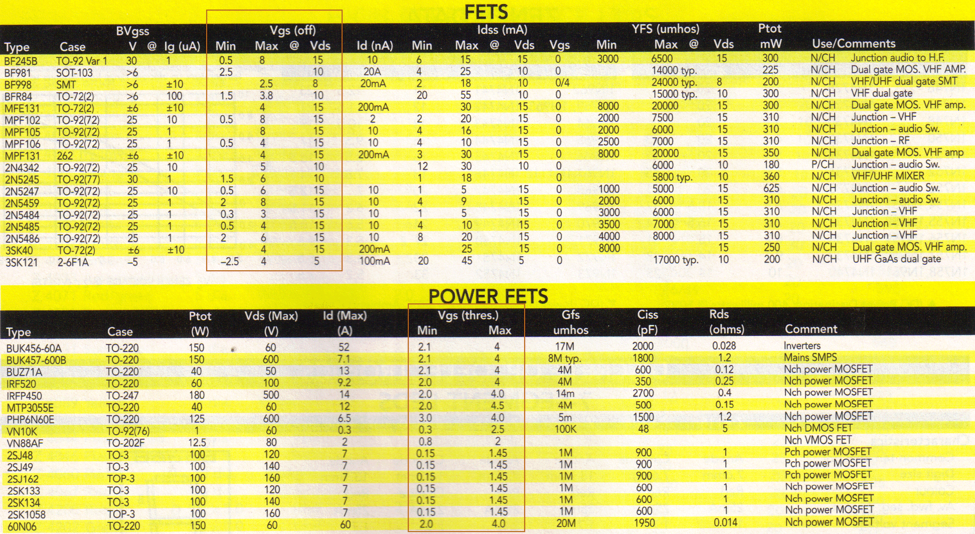


indeed very nice details with help of diagram i learn every thing This post is really very knowledgeable
Trả lờiXóaac
inverter ac
dc inverter ac